Quantcast
Channel: Ken Shirriff's blog
Viewing all 311 articles
Browse latest View live

Solving a math problem of Schrödinger with Arc and Python

$
0
0
I recently received an interesting math problem: how many 12-digit numbers can you make from the digits 1 through 5 if each digit must appear at least once. The problem seemed trivial at first, but it turned out to be more interesting than I expected, so I'm writing it up here. I was told the problem is in a book of Schrodinger's, but I don't know any more details of its origin.

(The problem came to me via Aardvark (vark.com), which is a service where you can send questions to random people, and random people send you questions. Aardvark tries to match up questions with people who may know the answer. I find it interesting to see the questions I receive.)

The brute force solution

I didn't see any obvious solution to the problem, so I figured I'd first use brute force. I didn't use the totally brute force solution - enumerating all 12 digit sequences and counting the valid ones - since it would be pretty slow, so I took a slightly less brute force approach.

If 1 appears a times, 2 appears b times, and 3, 4, and 5 appear c, d, and e times, then the total number of possibilities is 12!/(a!b!c!d!e!) - i.e. the multinomial coeffient.

Then we just need to sum across all the different combinations of a through e. a has to be at least 1, and can be at most 8 (in order to leave room for the other 4 digits). Then b has to be at least 1 and at most 9-a, and so on. Finally, e is whatever is left over.

The Python code is straightforward, noting that range(1, 9) counts from 1 to 8:

from math import factorial
total = 0
for a in range(1, 8+1):
  for b in range(1, 9-a+1):
    for c in range(1, 10-a-b+1):
      for d in range(1, 11-a-b-c+1):
        e = 12-a-b-c-d
        total += (factorial(12) / factorial(a) / factorial(b)
          / factorial(c) / factorial(d) / factorial(e))
print total
Or, in Arc:
(def factorial (n)
  (if (<= n 1) 1
     (* n (factorial (- n 1)))))

(let total 0
  (for a 1 8
    (for b 1 (- 9 a)
      (for c 1 (- 10 a b)
        (for d 1 (- 11 a b c)
          (let e (- 12 a b c d)
            (++ total (/ (factorial 12) (factorial a) (factorial b)
              (factorial c) (factorial d) (factorial e))))))))
  total)
Either way, we quickly get the answer 165528000.

The generalized brute force solution

The above solution is somewhat unsatisfying, since if we want to know how many 11 digits numbers can be made from at least one of 1 through 6, for instance, there's no easy way to generalize the code.

We can improve the solution by writing code to generate the vectors of arbitrary digits and length. In Python, we can use yield, which magically gives us the vectors one at a time. The vecs function recursively generates the vectors that sum to <= t. The solve routine adds the last entry in the vector to make the sum exactly equal the length. My multinomial function is perhaps overly fancy, using reduce to compute the factorials of all the denominator terms and multiply them together in one go.

from math import factorial

# Generate vectors of digits of length n with sum <= t, and minimum digit 1.
def vecs(n, t):
  if n <= 0:
    yield []
  else:
    for vec in vecs(n-1, t-1):
      for last in range(1, t - sum(vec) + 1):
        yield vec + [last]

def multinomial(n, ks):
  return factorial(n) / reduce(lambda prod, k: prod * factorial(k), ks, 1)
  
# Find number of sequences of digits 1 to n, of length len,
# with each digit appearing at least once
def solve(n, len):
  total = 0
  for vec0 in vecs(n-1, len-1):
    # Make the vector of length n summing exactly to len
    vec = vec0 + [len - sum(vec0)]
    total += multinomial(len, vec)
  return total
Now, solve(5, 12) solves the original problem, and we can easily solve related problems.

In Arc, doing yield would need some crazy continuation code, so I just accumulate the list of vectors with accum and then process it. The code is otherwise similar to the Python code:

(def vecs (n t)
  (if (<= n 0) '(())
    (accum accfn
      (each vec (vecs (- n 1) (- t 1))
       (for last 1 (- t (reduce + vec))
          (accfn (cons last vec)))))))

(def multinomial (n ks)
  (/ (factorial n) (reduce * (map factorial ks))))

(def solve (n len)
  (let total 0
    (each vec0 (vecs (- n 1) (- len 1))
        (++ total (multinomial len
                    (cons (- len (reduce + vec0)) vec0))))
    total))
This solution will solve our original problem quickly, but in general it's exponential, so solving something like n = 10 and length = 30 gets pretty slow.

The dynamic programming solution

By thinking about the problem a bit more, we can come up with a simpler solution. Let's take all the sequences of 1 through 5 of length 12 with each number appearing at least once, and call this value S(5, 12). How can we recursively find this value? Well, take a sequence and look at the last digit, say 5. Either 5 appears in the first 11 digits, or it doesn't. In the first case, the first 11 digits form a sequence of 1 through 5 of length 11 with each number appearing at least once. In the second case, the first 11 digits form a sequence of 1 through 4 of length 11 with each number appearing at least once. So we have S(5, 11) sequences of the first case, and S(4, 11) of the second case. We assumed the last digit was a 5, but everything works the same if it was a 1, 2, 3, or 4; there are 5 possibilities for the last digit.

The above shows that S(5, 12) = 5 * (S(5, 11) + S(4, 11)). In general, we have the nice recurrence S(n, len) = n * (S(n, len-1) + S(n-1, len-1)). Also, if you only have a single digit, there's only one solution, so S(1, len) = 1. And if you have more digits than length to put them in, there are clearly no solutions, so S(n, len) = 0 if n > len. We can code this up in a nice recursive solution with memoization:

memo = {}
def solve1(digits, length):
  if memo.has_key((digits, length)):
    return memo[(digits, length)]
  if digits > length:
    result = 0
  elif digits == 1:
    result = 1
  else:
    result = digits * (solve1(digits-1, length-1) + solve1(digits, length-1))
  memo[(digits, length)] = result
  return result
An interesting thing about this solution is it breaks down each function call into two simpler function calls. Each of these turns into two simpler function calls, and so forth, until it reaches the base case. This results in an exponential number of function calls. This isn't too bad for solving the original problem of length 12, but the run time rapidly gets way too slow.

Note that the actual number of different function evaluations is pretty small, but the same ones keep getting evaluated over and over exponentially often. The traditional way of fixing this is to use dynamic programming. In this approach, the structure of the algorithm is examined and each value is calculated just one, using previously-calculated values. In our case, we can evaluate S(1, 0), S(2, 0), S(3, 0), and so on. Then evaluate S(2, 1), S(2, 2), S(2, 3) using those values. Then evaluate S(3, 2), S(3, 3), and so on. Note that each evaluation only uses values that have already been calculated. For an introduction to dynamic programming, see Dynamic Programming Zoo Tour.

Rather than carefully looping over the sub-problems in the right order to implement a dynamic programming solution, it is much easier to just use memoization. The trick here is once a subproblem is solved, store the answer. If we need the answer again, just use the stored answer rather than recomputing it. Memoization is a huge performance win. Without memoization solve1(10, 30) takes about 15 seconds, and with it, the solution is almost immediate. (solve1 10 35) takes about 80 seconds.

The Arc implementation is nice, because defmemo creates a function that is automatically memoized.

(defmemo solve1 (digits length)
  (if (> digits length) 0
      (is digits 1) 1
      (* digits (+ (solve1 (- digits 1) (- length 1))
                   (solve1 digits (- length 1))))))

A faster dynamic programming solution

When trying to count the number of things satisfying a condition, it's often easier to figure out how many don't satisfy the condition. We can apply that strategy to this problem. The total number of 12-digit sequences made from 1 through 5 is obviously 5^12. We can just subtract the number of sequences that are missing one or more digits, and we get the answer we want.

How many sequences are missing 1 digit? S(4, 12) is the number of sequences containing at least one of 1 through 4, and by definition missing the digit 5. Of course, we need to consider sequences missing 4, 3, 2, or 1 as well. Likewise, there are S(4, 12) of each of these, so 5 * S(4, 12) sequences missing exactly one digit.

Next, sequences missing exactly 2 of the digits 1 through 5. S(3, 12) is the number of sequences containing at least one of 1 through 3, so they are missing 4 and 5. But we must also consider sequences missing 1 and 2, 1 and 3, and so on. There are 5 choose 2 pairs of digits that can be missing. Thus in total, (5 choose 2) * S(3, 12) sequences are missing exactly 2 of the digits.

Likewise, the number of sequences missing exactly 3 digits is (5 choose 3) * S(2, 12). The number of sequences missing exactly 4 digits is (5 choose 4) * S(1, 12). And obviously there are no sequences missing 5 digits.

Thus, we get the recurrence S(5, 12) = 5^12 - 5*S(4, 12) - 10*S(3, 12) - 10*S(2, 12) - 5*S(1, 12)

In general, we get the recurrence:

The same dynamic programming techniques and memoization can be applied to this. Note that the subproblems all have the same length, so there are many fewer subproblems than in the previous case. That is, instead of a 2-dimensional grid of subproblems, the subproblems are all in a single row.

In Python, the solution is:

memo = {}
def solve2(digits, length):
  if memo.has_key((digits, length)):
    return memo[(digits, length)]
  if digits > length:
    result = 0
  elif digits == 1:
    result = 1
  else:
    result = digits**length
    for i in range(1, digits):
      result -= sol2(i, length)*choose(digits, i)
  memo[(digits, length)] = result
  return result
And in Arc, the solution is similar. Instead of looping, I'm using a map and reduce just for variety. That is, the square brackets define a function to compute the choose and solve term. This is mapped over the range 1 to digits-1. Then the results are summed with reduce. As before, defmemo is used to memoize the results.
(def choose (m n)
  (/ (factorial m) (factorial n) (factorial (- m n))))

(defmemo solve2 (digits length)
  (if (> digits length) 0
      (is digits 1) 1
      (- (expt digits length)
         (reduce +
           (map [* (choose digits _) (solve2 _ length)]
             (range 1 (- digits 1)))))))

The mathematical exponential generating function solution

At this point, I dug out my old combinatorics textbook to figure out how to solve this problem. By using exponential generating functions and a bunch of algebra, we obtain a fairly tidy answer to the original problem:

Since the mathematics required to obtain this answer is somewhat complicated, I've written it up separately in Part II.

Discussion

This problem turned out to be a lot more involved than I thought. It gave me the opportunity to try out some new things in Python and Arc, and make use of my fading knowledge of combinatorics and generating functions.

The Python and Arc code was pretty similar. Python's yield construct was convenient. Arc's automatic memoization was also handy. On the whole, both languages were about equally powerful in solving these problems.

Acknowledgement: equations created through CodeCogs' equation editor


IPv6 web serving with Arc or Python: adventures in IPv6

$
0
0
Lego Minifig on a Sheevaplug running IPv6 I've been experimenting with IPv6 on my home network. In part 1, I described how I set up an IPv6 tunnel on Windows 7 and how IPv6 killed my computer. Now, I will describe how I set up a simple (i.e. trivial) IPv6 web server using Arc or Python, on Windows or Linux, which can be accessed at http://ipv6.nlanguages.com.

My IPv6 explorations are roughly driven by Hurricane Electric's IPv6 Certification levels. To get from "Newbie" to "Enthusiast" you have to have an IPv6 web server. I expected I could just use the web server you're viewing right now (provided through Pair), but Pair (like most web providers) doesn't support IPv6. So I figured I'd just set up my own simple web server.

To make things more interesting, I decided to set up the server on my Sheevaplug, a very small plug-based computer running Linux. (See my previous articles about Arc on the Sheevaplug, and Arduino with the Sheevaplug.) The things I describe will work just as well on a standard Linux or Windows box, though.

Setting up the SixXS IPv6 tunnel on the Sheevaplug was much easier than setting it up on Windows; I just followed the directions. One gotcha: if your clock is wrong, aiccu will silently fail - check /var/log/syslog.

IPv6 with the Python web server

Python comes with a simple web server. It is easy to configure the web server for IPv6 once you know how, but it took some effort to figure out how to do it.
import socket
from BaseHTTPServer import HTTPServer
from SimpleHTTPServer import SimpleHTTPRequestHandler

class MyHandler(SimpleHTTPRequestHandler):
  def do_GET(self):
    if self.path == '/ip':
      self.send_response(200)
      self.send_header('Content-type', 'text/html')
      self.end_headers()
      self.wfile.write('Your IP address is %s' % self.client_address[0])
      return
    else:
      return SimpleHTTPRequestHandler.do_GET(self)

class HTTPServerV6(HTTPServer):
  address_family = socket.AF_INET6

def main():
  server = HTTPServerV6(('::', 80), MyHandler)
  server.serve_forever()

if __name__ == '__main__':
  main()
Most of this code is standard Python SimpleHTTPServer code. It implements a handler for the path /ip, which returns the client's IP address. For other paths, SimpleHTTPRequestHandler returns a file from the current directory; this is not particulary secure, but works for a demonstration.

The key change to support IPv6 is subclassing HTTPServer and setting the address_family to IPv6. The other key change is starting the server with the name '::', which is the IPv6 equivalent of '', and binds to no specific address. Similar changes work with related Python classes such as SocketServer.

IPv6 with Arc's web server

My next adventure was to run Arc's web server (which I've documented here) on IPv6. Much to my surprise, Arc's web server worked on Windows with IPv6 without any trouble. You don't have to do anything different to serve on IPv6 and the code and logs handle IPv6 addresses as you'd expect. (Most of the credit for this should go to MzScheme/Racket, which provides the underlying socket implementation.)

I simply start a server thread on port 80, and then define a simple web operation on the home page (represented as || for obscure reasons).

arc> (thread (serve 80))
arc> (defop || req (pr "Welcome to Arc!  Your IP is " (req 'ip)))
Accessing this home page displays a message and the IP address of the client (IPv4 or IPv6 as appropriate).

Unfortunately, when I tried running the same Arc code on the Sheevaplug or another Linux box, it refused to work at all with IPv6. The problem turned out to be misconfiguration in the compilation of Racket (the new name for mzscheme). To get IPv6 working, you can recompile Racket following the instructions here. After recompiling, I was able to get Arc working on my Sheevaplug with IPv6. Eventually this fix will get into the official builds.

Note that implementing web pages in Arc requires much less boilerplate than in Python. This isn't too surprising, given that the primary application of Arc is web serving.

Putting the server's IPv6 address into DNS

Once you have an IPv6 web server, how do you access it? You can access a server with a raw IPv6 address: http://[2001:1938:81:1f8::2]/mypage. (Note that the IPv6 address is enclosed in square brackets, unlike a regular IP address.) However, you'll almost certainly want to access your IPv6 server through a domain name in DNS. To do this, you need to create an AAAA record in your domain zone file.

I had the domain name nlanguages.com available, and wanted to point it at my IPv6 web server. To do this, I went to the DNS Zone File Editor for my nameserver (godaddy.com in my case). I created one AAAA entry for host @ to point to my IPv6 address, and a second AAAA entry for host ipv6 to point to my IPv6 address. The @ provides an entry for my top-level domain (nlanguages.com), and the second provides an entry for ipv6.nlanguages.com. I then tested the DNS entries with a nslookup query, asking for the AAAA record: nslookup -q=aaaa nlanguages.com

The result is that http://ipv6.nlanguages.com will access my IPv6 server (if you have IPv6 access.)

Conclusion

Running a simple IPv6 web server in Python or Arc is straightforward, at least if you don't run into a problem with the underlying language implementation. Python requires just a couple additional lines to support IPv6, while Arc supports IPv6 automatically. Thus, you can easily set up an IPv6 web server, just in time for World IPv6 Day.

Solving a math problem of Schrödinger (Part II)

$
0
0
What's the better way to solve a math problem? A few lines of code, or a bunch of mathematical thought? I wanted to solve the following math problem: how many 12-digit numbers can you make from the digits 1 through 5 if each digit must appear at least once. In Part I, I described how to use Python or Arc to solve this problem. Now, in the eagerly-awaited Part II, I'll describe how to solve it using Exponential Generating Functions. This turned out to involve more mathematics than I expected, although it's mostly just algebra.

The exponential generating function solution

My old combinatorics textbook describes how to solve all sorts of combinatorial problems. Section 3.2.13 has a somewhat similar sequence problem: how many sequences of 1,2, or 3 of length l, in which no symbol occurs exactly p times. This approach can be generalized to the problem we're solving.

For our specific problem, we want to exclude solutions where a digit appears 0 times, but we'll stick with the generalized approach of excluding solutions where a digit appears exactly p times, and then we'll set p to 0 later. We'll let d be the range of each digit (e.g. if the digits are 1 through 5, then d=1). And n will be the total number of digits in the sequence (e.g. n=12 in our original problem).

Generating functions are way too complex to explain here, but I'll try to give a quick overview. The idea is that if you have c things of size n, you represent this by cx^n. For instance, if you roll a die, you can get 1 through 6, so the generating function would be x+x^2+x^3+x^4+x^5+x^6. If you roll a die twice, you would square that. If you want to figure out how many ways to roll a 9, you'd extract the coefficient of x^9 (which is represented as [x^9]). If you multiply out the polynomial, you'll find that the coefficient of x^9 is 4, corresponding to the 4 ways to roll a 9 (6+3, 5+4, 4+5, 3+6).

In these polynomials, x is just a placeholder, not a genuine variable; you never actually evaluate the polynomial. It's almost like magic the way the answer pops out of the formulas.

One source of more information on generating functions is Cut the knot: generating functions.

First, we create the generating function for a single digit, say 1. If the digit appears zero times, we represent it by term x^0. If it appears 1 time, we have x^1. If it appears twice, we have x^2/2!. (We divide by 2! because there are 2! equivalent ways the digit can appear twice.) Likewise, if it appears three times, we represent it by x^3/3!. We end up with x^0 + x^1 + x^2/2! + x^3/3! + x^4/4! + ... Now for the crazy part. This is the series expansion of e^x, so we replace this with e^x. Finally we subtract x^p/p!, which is the "forbidden" case. We end up with the generating function e^x - x^p/p!.

If we have d choices for each digit, we multiply together d copies of the generating function, which is of course raising it to the power of d:

To get our solution, if we want to find how many solutions are n digits long, we simply extract the coefficient of x^n/n! from the above generating function, and that gives us the value we want:

Next step: how do we evaluate the above? First, let's expand the right half using the standard binomial formula:

Now we'll take a quick detour through some generating function facts, which I will present without proof.

Important generating function facts

Extracting the coefficient of x^n in an exponential gives you:

Unless n=0. Then you're looking for the coefficient of x^n in 1. This is simply 1 if n=0, and 0 otherwise.

Or unless n<0. Then the result is 0.

Second important generating function fact: if you're looking for the coefficient of, say, x^9 in an expression multiplied by x^3, then you can look instead for the coefficient of x^6 in the expression, if you use the appropriate scaling:

Solving one term of the summation

Now let's extract our desired coefficient from one term of the summation.

If n<kp, then the coefficient is 0.

If d != k, then from the second important fact, the value is:

If k = d, then the exponential drops out and the value is 0 if n != kp (i.e. n != dp), and otherwise:

Putting the summation together

Let's first assume n != dp. Then we can skip the k=d term, and we get:

where limit = min(d-1, n/p) (or d-1 if p=0). This ensures that n-kp >=0.

On the other hand, if n = dp, then we need to handle the k=d term.

Note that if n=dp, then n-kp>0, so we don't need to add an extra upper limit on k.

Solving the original problem

In the original problem, no value is allowed to appear zero times, so the forbidden count p=0. Then the solution simplifies to

Thus, the number of sequences of length 12 consisting of the digits 1 through 5, with each digit appearing at least once, is given by n=12 and d=5:

Happily, this is the same result we got in Part I.

Implementing this in Python

Implementing the above formula is straightforward:
from math import factorial

def solve(d, n, p):
  total = 0
  for k in range(0, d):
    if n-k*p < 0: break
    total += (pow(-1, k) * choose(d, k) *
              factorial(n) / factorial(n-k*p) *
              pow(d-k, n-k*p) / pow(factorial(p), k))
  if n == d*p:
    total += pow(-1, d) * factorial(n) / pow(factorial(p), d)
  return total
Since I didn't entirely trust the mathematics above, I also implemented a totally brute-force solution that generates and tests all the sequences of the given length:
import itertools

def bruteforce(d, n, p):
  total = 0
  for seq in itertools.product(range(0, d), repeat=n):
    ok = 1
    for i in range(0, d):
      if len([x for x in seq if x==i]) == p:
        ok = 0
        break
    total += ok
  return total
The mathematical solution and the brute force solution agree on the cases I tested, which increased my confidence that I didn't mess up the math. The brute force solution is, of course, too slow to use except for fairly small values.

Conclusion

The mathematical solution involved more mathematics than I was expecting. The resulting solution isn't quite as clean as I'd hoped, due to various corner cases that need to be handled. But it can be implemented fairly easily, and also lets us solve a more general problem than the original problem.

The Endeavour delay: Complexity, the APU, and the Load Control Assembly

$
0
0
The last launch of the Endeavour space shuttle has been delayed 48 hours (update: indefinitely) due to a problem with the APU heater and the Load Control Assembly. I wanted to find out what exactly these troublesome components are, so I did some investigation. There's a lot of extremely detailed information on the Space Shuttle available online, but it is very hard to find. I've summarized the information here in case anyone else wants to know the specifics.

Space Shuttle APU locations

The Space Shuttle has three independent hydraulic systems to operate engine valves, actuators, landing gear, and so forth during launch and landing. The hydraulic pumps are powered by three Auxiliary Power Units (or APUs), which are hydrazine-powered turbines. Each APU is 88 pounds and produces 135 horsepower (which is about the same horsepower as a Honda Accord).

Hydrazine is a highly-toxic rocket fuel; when exposed to a catalyst, it energetically decomposes into hot gases at 1700°F. It is convenient for applications such as the APU, since it doesn't need oxygen, and the decomposition can be easily started and stopped.

Space Shuttle Auxiliary Power Unit
(Click on the image for tons of detailed information.)

Apparently the fuel heaters in APU 1 are not working. Since the hydrazine fuel will freeze at 34°F, each APU has redundant heaters to keep the system above 45°F. Since the heaters are redundant, the Space Shuttle would still be able to operate with the current problem, but would not be able to handle another failure. If the second fuel heater failed, then the fuel would freeze and the APU would not be able to work. Since there are three APUs, even this failure would not be a major problem. But still, you wouldn't want to take off with the heater not working, because losing hydraulic pressure would be a very bad thing.

According to articles, the fuel heater problem is due to a lack of power from the Aft Cabin Load Control Assembly, a switchbox that powers a heater circuit for Auxiliary Power Unit 1. There are three Aft Load Controller Assemblies, as well as many other Load Controller Assemblies. (Sources are inconsistent about whether it is called a Control vs Controller.)

A complex Electrical Power System provides power to all parts of the Shuttle. Three fuel cells (10 kW each) generate 28-volt direct current. The fuel cells feed three main DC power buses, as well as powering AC inverters to feed three AC buses with three-phase, 117-volt, 400-hertz AC power. From the fuel cell, power goes to a Distribution Assembly (DA), then to the aft Power Controller Assemblies, and then to the Aft Load Controller Assemblies.

The Load Control Assemblies contain solid-state switching devices for loads up to 20 amps, and relays for loads up to 135 amps. These switching devices are internally fused.

Reportedly there is a short or other electrical fault in the Aft Load Controller Assembly 2, which is causing the APU heater to fail to operate. The fuel is being drained from Endeavour so technicians can access the assembly and resolve the problem. If I'm interpreting everything correctly, it seems like they'll need to replace one of the internal fuses in the Load Control Assembly.

Space Shuttle Power Distribution

Complexity and the Space Shuttle

One amazing thing about the Space Shuttle is the layers and layers of complexity. The APU system is just one example of this. For instance, each APU has as lube oil system to keep it lubricated. This requires a lube oil pump, which requires a nitrogen pressurization system to start the pump in zero gravity. The oil also requires a 181-pound water spray boiler system, which sprays cooling water onto the oil pipes; the water boils into steam and is vented into space. The boiler requires controllers, panel switches, and status displays, as well as yet another nitrogen pressurization tank, and yet another system of heaters to keep the water from freezing.

Space Shuttle Water Spray Boiler

The water spray boiler doesn't have anything to do with the current launch delay, other than being part of the APU, but it provides an interesting example of the complexity of the systems involved. To summarize the complexity along just this one path, the engines require hydraulic pressure, which requires APUs to power the hydraulic pumps, which require a lubricating oil system, which requires a complex boiler system, which requires a own control and monitoring system. And this is just one small sub-path! I'm ignoring equally complex systems such as the APU injector cooling system (more water and pressurized nitrogen), or the APU fuel pump (which for instance, has a catch bottle in case its seals leak, a drain port if the catch bottle overflows, and associated monitoring system).

Conclusion

Given the level of complexity of the Space Shuttle, I'm not surprised by the launch delays, and wish NASA the best of luck in resolving the problem promptly. My opinion is while the Space Shuttle is a marvel of engineering, simpler rocket systems such as the SpaceX Falcon will turn out to be more practical in the long run.

The images and much of the information above is from the 1988 Shuttle Reference Manual at shuttlepresskit.com. This manual goes into extreme detail and is very interesting (if you find this sort of thing interesting). I should probably make it clear that this posting is based on what I've read; I have no connection with the space program.

P.S. I've found extensive details on the LCA and launch issues are available at nasaspaceflight.com, e.g. Endeavour receives her new LCA – Blown driver examined.

My Knuth reward check

$
0
0
I attended a very interesting talk "All Questions Answered" by the famous computer science professor Don Knuth in March, where he talked about many things, including his new book.

The talk inspired me to read The Art of Computer Programming, Volume 4A: Combinatorial Algorithms. As he described in the talk, he gives a reward check (for 1 hexadecimal dollar) to anyone who finds an error in one of his books, so I set myself the goal of finding an error in the book while on vacation.

After a lot of study, I thought I'd found an error in a diagram, but then I realized I was confused. Next, I found a blatant error in an appendix, but that error had already been discovered and was listed in the errata. Finally I found an error on page 574 that I hoped hadn't been found yet and sent it off to Professor Knuth.

I was delighted to receive my reward check today, which Wikipedia calls "among computerdom's most prized trophies". That's a big exaggeration but nonetheless, I'm happy to get one. Note that the check is from the fictional Bank of San Seriffe to avoid check fraud problems from all the images of his checks on the web.

My Knuth TAOCP reward check

As for the book itself, it's interesting even if you're not after a reward, although very challenging to read. Volume 4a describes combinatorial algorithms, including more ways of computing permutations and combinations than you can shake a stick at. It also has an extensive discussion of BDDs and ZDDs, which are newish data structures for representing sets. The section on bitwise tricks and techniques is interesting if you like HAKMEM-style tricks such as reversing the bits in an integer through a short sequence of incomprehensible operations.

I have to admit that trying to find an error in a book is a strange vacation goal, but I'm glad I succeeded and Knuth's book taught me some interesting algorithms in the process.

P.S. I was very surprised to see this article on the front page of Hacker News. To answer the questions there and below, the error I found was in volume 4a page 574 (as the memo line on the check shows). The solution to exercise 67 on that page says a particular circuit uses 6 ANDN gates, which I thought should be NAND gates. It gets a bit more complicated because Knuth was referring to the ANDN op code for MMIX, but there was still a mistake with and-not versus not-and. (The other error I noticed was n choose k on page 824, but I checked the errata and it had already been found.)

My 0.015 minutes of fame on CNN

$
0
0
I recently wound up on CNN for a couple seconds doing some Arduino hacking as part of a segment on Google's workshops. Click the image for the full video. If you don't want to watch the whole thing, I appear at 1:00 and 1:39.

Ken Shirriff on CNN

For those who want technical details, I hacked together the following quick sketch to generate the interesting patterns you can see on the oscilloscope:

void setup()
{
  pinMode(4, OUTPUT);
  pinMode(5, OUTPUT);
}

int state = 1;
int count1 = 0;
int state2 = 1;
int count12 = 0;
int max1 = 20;
int max2 = 200;
int t = 0;

void loop() {

  if (count1-- <= 0) {
    state = 1-state;
    digitalWrite(5, state);
    count1 = max1;
  }
  if (count12-- <= 0) {
    state2 = 1-state2;
    digitalWrite(4, state2);
    count12 = max2;

    if (t++ > 20000) {
      max2 -= 1;
      if (max2 < 1) {
        max2 = 500;
      }   
      t = 0;
    }
  }
}
This sketch manually generates two square wave output with periods determined by max1 and max2. The frequency of the second varies occasionally (controlled by the loop with t). I used simple R-C filters on the outputs to turn the square waves into roughly triangular waves, and then fed this into the X and Y inputs of the oscilloscope. The result was constantly-varying Lissajou-like patterns.

I should point out the outputs generated this way are rather unstable because many thing can interrupt the timing loop. The above code is provided just in case your are curious. I don't recommend using this approach for anything real; using the PWM timers would yield much cleaner results.

Anyone have other ideas for easy ways to generate cool oscilloscope patterns with an Arduino?

The Mathematics of Volleyball

$
0
0
Recently I was at a multi-day volleyball tournament, which gave me plenty of time to ponder the mathematics of the game. At different points in the game, I'd wonder what the odds were of each team winning. And when a team gained or lost a point, I'd wonder how important that point was. Clearly, if the score was 24-24, gaining a point made a huge difference. But how much difference did getting one point at the beginning of the game matter? It seemed like it didn't matter much, but did it?

I decided to analyze the game mathematically. I made the simplifying assumption that each team had 50-50 odds of winning each point. I found the analysis interesting, and it turns out to have close ties to Pascal's Triangle, so I'm posting it here in case anyone else is interested.

Volleyball games are scored using the rally point system, which means that one team gets a point on every serve. (Back in the olden days, volleyball used side-out scoring, which meant that only the serving team could get a point. Fortunately, rally point scoring is more mathematically tractable. Rally point scoring also keeps the game advancing faster.) The winner of each match is the best out of three sets (a set is the same as a game). In the league I was watching, the winner of a game is the first team to get 25 points and be ahead by at least 2. (Except if a third tiebreaker game is needed, it only goes to 15 points instead of 25.)

A few cases are easy to analyze mathematically. If we assume each team has a 50-50 chance of scoring each point and the score is tied, each team obviously has a 50% chance of winning the game. (With side-out scoring, it makes a difference which team is serving, but for rally point scoring we avoid that complication.) The second obvious case is if a team has 25 points and the other team has 23 or fewer points, the first team has 100% chance of winning (since they already won).

I will use the notation P(m,n) for the chance of the first team wining if the score is m to n. From above, P(n, n) = 50%, P(25, n) = 100% for n <= 23, and P(m, 25) = 0% for m <= 23.

The chance of winning in other cases can be calculated from the assumption that a team has a 50% chance of winning the point, and a 50% chance of losing: the chance of winning is the average of these two circumstances. Mathematically, we get the simple recurrence:

For instance, if the score is 25-24, if the first team scores, they win. If the second team scores, then the score is tied. In the first (winning) case, the first team wins 100%, and in the second (tied) case, the first team wins 50%. Thus, on average they will win 75% of the time from a 25-24 lead. That is, P(25, 24) = 75%, and by symmetry P(24, 25) = 25%. (Surprisingly, these are the only scores where the requirement to win by 2 points changes the odds.)

Likewise, if the score is 24-23, half the time the first team will score a point and win, and half the time the second team will score a point and tie. So the first team has 1/2 * 100% + 1/2 * 50% = 75% chance of winning, and P(24, 23) = 75%.

More interesting is if the score is 24-22, half the time the first team will score a point and win, and half the time the second team will score, making the score 24-23. We know from above that the first team has a 75% chance of winning from 24-23, so P(24, 22) = 1/2 * 100% + 1/2 * 75% = 87.5%.

We can use the recurrence to work backwards and find the probability of winning from any score. The following table shows the probability of winning for each score. The first team has the score on the left, and the second team has the score on the top.

Table with odds of winning when the score is m to n

012345678910111213141516171819202122232425
050%44%39%33%28%23%18%14%11%8%5%4%2%1%1%0%0%0%0%0%0%0%0%0%0%0%
156%50%44%38%33%27%22%17%13%10%7%5%3%2%1%1%0%0%0%0%0%0%0%0%0%0%
261%56%50%44%38%32%27%21%17%13%9%7%4%3%2%1%1%0%0%0%0%0%0%0%0%0%
367%62%56%50%44%38%32%26%21%16%12%9%6%4%3%1%1%0%0%0%0%0%0%0%0%0%
472%67%62%56%50%44%37%31%26%20%16%11%8%6%4%2%1%1%0%0%0%0%0%0%0%0%
577%73%68%62%56%50%44%37%31%25%20%15%11%7%5%3%2%1%0%0%0%0%0%0%0%0%
682%78%73%68%63%56%50%43%37%30%24%19%14%10%7%4%3%1%1%0%0%0%0%0%0%0%
786%83%79%74%69%63%57%50%43%36%30%24%18%13%9%6%4%2%1%1%0%0%0%0%0%0%
889%87%83%79%74%69%63%57%50%43%36%29%23%17%12%8%5%3%2%1%0%0%0%0%0%0%
992%90%87%84%80%75%70%64%57%50%43%36%29%22%16%11%8%5%3%1%1%0%0%0%0%0%
1095%93%91%88%84%80%76%70%64%57%50%43%35%28%21%15%11%7%4%2%1%0%0%0%0%0%
1196%95%93%91%89%85%81%76%71%64%57%50%42%35%27%20%14%9%6%3%2%1%0%0%0%0%
1298%97%96%94%92%89%86%82%77%71%65%58%50%42%34%26%19%13%8%5%2%1%0%0%0%0%
1399%98%97%96%94%93%90%87%83%78%72%65%58%50%42%33%25%18%12%7%4%2%1%0%0%0%
1499%99%98%97%96%95%93%91%88%84%79%73%66%58%50%41%32%24%17%11%6%3%1%0%0%0%
15100%99%99%99%98%97%96%94%92%89%85%80%74%67%59%50%41%31%23%15%9%5%2%1%0%0%
16100%100%99%99%99%98%97%96%95%92%89%86%81%75%68%59%50%40%30%21%13%7%3%1%0%0%
17100%100%100%100%99%99%99%98%97%95%93%91%87%82%76%69%60%50%40%29%19%11%5%2%0%0%
18100%100%100%100%100%100%99%99%98%97%96%94%92%88%83%77%70%60%50%39%27%17%9%4%1%0%
19100%100%100%100%100%100%100%99%99%99%98%97%95%93%89%85%79%71%61%50%38%25%14%6%2%0%
20100%100%100%100%100%100%100%100%100%99%99%98%98%96%94%91%87%81%73%62%50%36%23%11%3%0%
21100%100%100%100%100%100%100%100%100%100%100%99%99%98%97%95%93%89%83%75%64%50%34%19%6%0%
22100%100%100%100%100%100%100%100%100%100%100%100%100%99%99%98%97%95%91%86%77%66%50%31%12%0%
23100%100%100%100%100%100%100%100%100%100%100%100%100%100%100%99%99%98%96%94%89%81%69%50%25%0%
24100%100%100%100%100%100%100%100%100%100%100%100%100%100%100%100%100%100%99%98%97%94%88%75%50%25%
25100%100%100%100%100%100%100%100%100%100%100%100%100%100%100%100%100%100%100%100%100%100%100%100%75%50%

Any particular chance of winning can be easily read from the table. For instance, if the score is 15-7, look where row 15 and column 7 meet, and you'll find that the first team has a 94% chance of winning. (This is P(15, 7) in my notation.)

The table illustrates several interesting characteristics of scores. The odds fall away from 50% pretty rapidly as you move away from the diagonal (i.e. away from a tied score). Points matter a lot more near the end of the game, though: you've only got a 1% chance of winning from an 18-24 position, while being six points behind at the beginning (0-6) still gives you an 18% chance of winning. However, a big deficit is almost insurmountable - if you're behind 0-15, you have less than a 1% chance of catching up and winning. (Note that 0% and 100% in the table are not exactly 0% and 100%, because there's always some chance to win or lose.)

Note that each score is the average of the score below and the score to the right - these are the cases where the first team gets the point and the second team gets the point. This corresponds directly to the equation above.

The table could be extended arbitrarily far if neither team gets a two point lead, but those cases are not particularly interesting.

Generating the score table with dynamic programming

To generate the table, I wrote a simple Arc program to solve the recurrence equation using dynamic programming:
(def scorePercent (s1 s2 max)
  (if (and (>= s1 max) (>= s1 (+ s2 2))) 100.
      (and (>= s2 max) (>= s2 (+ s1 2))) 0
      (is s1 s2) 50.
      (/ (+ (scorePercent s1 (+ s2 1) max)
            (scorePercent (+ s1 1) s2 max)) 2)))
The first two arguments are the current score, and the last argument is the amount to win (25 in this case). For instance:
arc> (scorePercent 24 22 25)
87.5
arc> (scorePercent 20 22 25)
22.65625
Unfortunately, the straightforward way of solving the problem has a severe performance problem. For instance, omputing (scorePercent 5 7 25) takes hours and hours. The problem is that evaluating P(5, 7) requires calculating two cases: P(6, 7) and P(5, 8). Each of those requires two cases, each of which requires two cases, and so on. The result is an exponential number of evaluations, which takes a very very long time as the scores get lower. Most of these evaluations calculate the same values over and over, which is just wasted work. For instance, P(6, 8) is computed in order to compute P(6, 7) and P(6, 8) is computed again in order to compute P(5, 8).

There are a couple ways to improve performance. The hard way of solving the dynamic programming problem without this exponential blowup is to carefully determine an order in which each value can be calculated exactly once by working backwards, until you end up with the desired value. For instance, if the values are calculated going up the columns from right to left, each value can be computed immediately from two values that have already been computed, until we end up efficiently computing the whole table in approximately 25*25 steps. This requires careful coding to step through the table in the right order and to save each result as it is calculated. It's not too hard, but there's a much easier way.

The easy way of solving the problem is with memoization - when an intermediate value is calculated, remember its value in case you need it again, instead of calculating it over and over. With memoization, we can compute the results in any order we want, and automatically each result will only be computed once.

In Arc, memoization can be implemented simply by defining a function with defmemo, which will automatically memoize the results of the function evaluation:

(defmemo scorePercent (s1 s2 max)
  (if (and (>= s1 max) (>= s1 (+ s2 2))) 100.
      (and (>= s2 max) (>= s2 (+ s1 2))) 0
      (is s1 s2) 50.
      (/ (+ (scorePercent s1 (+ s2 1) max)
            (scorePercent (+ s1 1) s2 max)) 2)))
With this simple change, results are nearly instantaneous, rather than taking hours.

The above function generates a single entry in the table. To generate the full table in HTML with colored cells, I used a simple loop and Arc's HTML generating operations. If you're interested in Arc programming, the full code can be downloaded here.

Mathematical analysis

Instead of computing the probabilities through dynamic programming, it is possible to come up with a mathematical solution. After studying the values for a while, I realized rather surprisingly that the probabilities are closely tied to Pascal's Triangle. You may be familiar with Pascal's Triangle, where each element is the sum of the two elements above it (with 1's along the edges), forming a table of binomial coefficients:

Pascal's Triangle

Pascal's triangle

The game probabilities come from the triangle of partial sums of binomial coefficients, which is a lesser-known sequence that is easily derived from Pascal's Triangle. This sequence, T(n, k) is formed by summing the first k elements in the corresponding row of Pascal's Triangle. That is, the first element is the first element in the same row of Pascal's triangle, the second is the sum of the first two elements in Pascal's triangle, the third is the sum of the first three, etc.

T - the partial row sums of Pascal's Triangle

Partial row sums in Pascal's triangle
Mathematically, this triangle T(n, k) is defined by:


As with Pascal's Triangle, each element is the sum of the two above it, but now the right-hand border is powers of 2. This triangle is discussed in detail in the Online Encyclopedia of Integer Sequences. Surprisingly, this triangle is closely connected with distances in a hypercube, error-correcting codes, and how many pieces an n-dimensional cake can be cut into.

With function T defined above, the volleyball winning probabilities are given simply by:

For example, P(23,20) = T(6, 4)/2^6 = 89.0625%, which matches the table.

Intuitively, it makes sense that the probabilities are related to Pascal's Triangle, because each entry in Pascal's Triangle is the sum of the two values above, while each probability entry is the average of the value above and the value to the right in the table. Because taking the average divides by 2 in each step, an exponent of 2 appears in the denominator. The equation can be proved straightfowardly by induction.

The importance of a point

Suppose the score is m to n. How important is the next point? I'll consider the importance of the point to be how much more likely the team is to win the game if they win the point versus losing the point. For instance, suppose the score is 18-12, so the first team has a 92% chance of winning (from the previous table). If they win the next point, their chance goes up to 95%, while if they lose the point, their chance drops to 88%. Thus, we'll consider the importance to be 7%. Mathematically, if the score is m to n, I define the importance as P(m+1, n) - P(m, n+1).

Table with importance of the next point when the score is m to n

012345678910111213141516171819202122232425
011%11%11%11%10%9%8%7%6%5%4%3%2%1%1%0%0%0%0%0%0%0%0%0%0%0%
111%12%12%11%11%10%9%8%7%6%4%3%2%2%1%1%0%0%0%0%0%0%0%0%0%0%
211%12%12%12%12%11%10%9%8%7%6%4%3%2%2%1%1%0%0%0%0%0%0%0%0%0%
311%11%12%12%12%12%11%10%9%8%7%5%4%3%2%1%1%0%0%0%0%0%0%0%0%0%
410%11%12%12%13%13%12%12%11%9%8%7%5%4%3%2%1%1%0%0%0%0%0%0%0%0%
59%10%11%12%13%13%13%13%12%11%10%8%7%5%4%3%2%1%1%0%0%0%0%0%0%0%
68%9%10%11%12%13%13%13%13%12%11%10%8%6%5%3%2%1%1%0%0%0%0%0%0%0%
77%8%9%10%12%13%13%14%14%13%12%11%10%8%6%5%3%2%1%1%0%0%0%0%0%0%
86%7%8%9%11%12%13%14%14%14%14%13%11%10%8%6%4%3%2%1%0%0%0%0%0%0%
95%6%7%8%9%11%12%13%14%14%14%14%13%12%10%8%6%4%3%1%1%0%0%0%0%0%
104%4%6%7%8%10%11%12%14%14%15%15%14%13%12%10%8%6%4%2%1%1%0%0%0%0%
113%3%4%5%7%8%10%11%13%14%15%15%15%15%14%12%10%7%5%3%2%1%0%0%0%0%
122%2%3%4%5%7%8%10%11%13%14%15%16%16%15%14%12%10%7%5%3%1%1%0%0%0%
131%2%2%3%4%5%6%8%10%12%13%15%16%17%17%16%14%12%9%7%4%2%1%0%0%0%
141%1%2%2%3%4%5%6%8%10%12%14%15%17%18%18%17%15%12%9%6%3%2%1%0%0%
150%1%1%1%2%3%3%5%6%8%10%12%14%16%18%19%19%17%15%12%9%5%3%1%0%0%
160%0%1%1%1%2%2%3%4%6%8%10%12%14%17%19%20%20%18%16%12%8%4%2%0%0%
170%0%0%0%1%1%1%2%3%4%6%7%10%12%15%17%20%21%21%19%16%12%7%3%1%0%
180%0%0%0%0%1%1%1%2%3%4%5%7%9%12%15%18%21%23%23%21%16%11%5%2%0%
190%0%0%0%0%0%0%1%1%1%2%3%5%7%9%12%16%19%23%25%25%22%16%9%3%0%
200%0%0%0%0%0%0%0%0%1%1%2%3%4%6%9%12%16%21%25%27%27%23%16%6%0%
210%0%0%0%0%0%0%0%0%0%1%1%1%2%3%5%8%12%16%22%27%31%31%25%12%0%
220%0%0%0%0%0%0%0%0%0%0%0%1%1%2%3%4%7%11%16%23%31%38%38%25%0%
230%0%0%0%0%0%0%0%0%0%0%0%0%0%1%1%2%3%5%9%16%25%38%50%50%25%
240%0%0%0%0%0%0%0%0%0%0%0%0%0%0%0%0%1%2%3%6%12%25%50%50%50%
250%0%0%0%0%0%0%0%0%0%0%0%0%0%0%0%0%0%0%0%0%0%0%25%50%50%

The values in the table make intuitive sense. If one team is winning by a lot, one more point doesn't make much difference. But if the scores are close, then each point counts. Each point counts a lot more near the end of the game than at the beginning. The first point only makes an 11% difference in the odds of winning, while the if the score is 23-23, the point makes a 50% difference (75% chance of winning if you get the point vs 25% if you miss the point). This table is sort of a derivative of the first table, showing where the values are changing most rapidly.

The importance of a point as defined above closely matches the behavior of the spectators. If the score is very close at the end of the game, the audience becomes much more animated compared to earlier in the game.

The "importance" is mathematically simpler than the probability of winning derived earlier. If the current score is 25-a, 25-b, then the importance is given by the simple equation:

This can proved straighforwardly from the equation for P(x, y). For example, if the score is 18-12, the importance is C(7+13-2, 6) / 2^(7+13-2) = 18564 / 262144 = 7.08%.

Conclusions

How useful is this model? Well, it depends on the assumption that each team has an equal chance of winning each point. Of course, most teams are not evenly matched. Even more important is the fact that if a team has a good server, they can quickly rack up 10 points in a row, which throws the model out the window.

However, I think the model is still useful, since it provides some quantitative answers to the original questions, and confirms some intuitions. In addition, the mathematics turned out to be more interesting than I was expecting, with the surprising connection to Pascal's Triangle.

Cells are very fast and crowded places

$
0
0
I recently learned that cells are extremely crowded and busy places. I knew there's a lot of activity in cells, but I didn't realize just how much until I was reading Molecular Biology of the Cell. I was reading this molecular biology textbook to find out what's happened in molecular biology in the last decade or so, and found I had some misconceptions about how fast things happen inside cells.

You may have seen the amazing "Inner Life of a Cell" video, which has spectacular animations of the activities inside a cell as a whilte blood cell responding to inflammation. (There's also a longer narrated version at the BioVisions website.)

Cells are very crowded

I imagined cells as big open spaces with lots of stuff happening, perhaps something like Central Park. From the "Inner Life of a Cell" video, or the typical drawing of a cell, it looks like a lot of empty space. But it turns out that cells are crammed full of stuff, more like New Year's Eve at Times Squares. Proteins are packed tightly into cells. The following picture is a representation of how crowded cells really are, with blue RNAs, green ribosomes, and red proteins.
Image: "The structure of the cytoplasm" from Molecular Biology of the Cell. Adapted from D.S. Goodsell, Trends Biochem. Sci. 16:203-206, 1991.
I came across another interesting representation of how crowded cells are. This diagram shows a synaptic vesicle, which is the part of a neuron that releases neurotransmitters from one neuron to another. When I saw this diagram, I assumed that the authors crammed all the different proteins into the picture so they could create a nice illustration of the different membrane proteins. But in fact, the diagram below omits 1/3 of the proteins so real membranes are even more crowded. The paper containing this diagram states that instead of thinking of membranes with proteins floating in them like icebergs, we should think of membranes as packed with proteins like a cobblestone pavement.
A neural vesicle studded with proteins
Image: "Molecular Model of an Average SV" from Molecular Anatomy of a Trafficking Organelle, Takamori et al, Cell. 2006 Nov 17;127(4):831-46.

Molecules move very very fast

You may wonder how things get around inside cells if they are so crowded. It turns out that molecules move unimaginably quickly due to thermal motion. A small molecule such as glucose is cruising around a cell at about 250 miles per hour, while a large protein molecule is moving at 20 miles per hour. Note that these are actual speeds inside the cell, not scaled-up speeds. I'm not talking about driving through a crowded Times Square at 20 miles per hour; to scale this would be more like driving through Times Square at 20 million miles per hour!

Because cells are so crowded, molecules can't get very far without colliding with something. In fact, a molecule will collide with something billions of times a second and bounce off in a different direction. Because of this, molecules are doing a random walk through the cell and diffusing all around. A small molecule can get from one side of a cell to the other in 1/5 of a second.

As a result of all this random motion, a typical enzyme can collide with something to react with 500,000 times every second. Watching the video, you might wonder how the different pieces just happen to move to the right place. In reality, they are covering so much ground in the cell so fast that they will be in the "right place" very frequently just by chance.

In addition, a typical protein is tumbling around, a million times per second. Imagine proteins crammed together, each rotating at 60 million RPM, with molecules slamming into them billions of times a second. This is what's going on inside a cell.

I'm not blaming the makers of "Inner Life of a Cell" for slowing down the action in a cell. If the video were totally realistic, you wouldn't see anything, since the action would be too fast to even see a blur. But keeping the real speed of the cell in mind can clear up a lot of things, such as how molecules find their way around.

The incredible speed and density of cells also helps explain why it's so difficult to simulate what's happening inside a cell. Even with a supercomputer, there's way too much going on inside a cell to simulate it without major simplifications. Even simulating a single ribosome is a huge computational challenge.

Molecular motors sprint, not walk

Another thing that surprised me about cells is how fast the motors inside cells move. Like a mechanical robot with two lumbering feet, a kinesin motor protein can be seen in the video at the 2 minute mark dragging a monstrous bag-like vesicle along a microtubule track. (This should be what you see in the YouTube preview frame at the top of the page.) These motor proteins move cargo through the cell if diffusion isn't fast enough to get things to their destination, which is especially important in extremely long cells such as neurons. Kinesin motors also help separate cells that are dividing.

It's remarkable enough that cells contain these mechanical walkers, but I recently learned that they aren't plodding along, but actually sprint at 100 steps per second. If you watch the video again, imagine it sped up to that rate.

Cells are powered by electric motors spinning at 40,000 rpm

Mitochondria also provide a fascinating look at just how fast things are inside cells. You may know that mitochondria are the power plants of cells; they take in food molecules, process it through the famous citric acid cycle, and then use oxygen to extract more energy, which is provided to the rest of the cell through molecules of ATP, the cell's "energy currency".

Image from David Goodsell, ATP Synthase, December 2005 Molecule of the Month
Mitochondria have many strange features - such as their own DNA separate from the cell's - but one of their strangest features is they use electric motors to produce ATP. Mitochondria use the energy from oxidizing food to pump protons out of the cell, creating a voltage of 170mV across the cell. This voltage causes a complex enzyme to spin, and the mechanical energy of this spinning enzyme creates the ATP molecules that energize the rest of the cell.

The same Harvard group that created "Inner Life of a Cell" also created a two minute sequel, "Powering the Cell: Mitochondria", which shows mitochondria in action. Around the 1:10 mark, the video shows the rotating ATP synthase enzymes creating glowing ATP molecules.

Watching the leisurely turning enzymes illustrates one of the amazingly complex mechanisms in a cell. But what really surprised me was to learn that in real life, these enzymes spin at up to 700 revolutions per second, which is faster than a jet engine. As I said earlier, cells are really, really fast.

If you're interested in more about this mechanical motor, you'll probably enjoy PDB's molecule of the month article.

Conclusions

The molecules inside a cell are moving almost unimaginably fast. Understanding this speed helped me compreshend how cells could carry out all their tasks, and how the different components of a cell could manage to be in the right place at the right time.

The BioVisions videos are very interesting, and I highly recommend watching them. (I also found Molecular Biology of the Cell very interesting and readable, but as it is a 1200+ page text, I don't imagine many people would read it unless they had to. But if you're still reading this article, maybe you're one of those people.)


A new multi-branch algorithm to render rational-exponent Mandelbrot fractals: Part I

$
0
0
If you came here from Hacker News, thanks for visiting. You might want to check out the Hacker News comment thread too.

The Mandelbrot fractal is generated by repeatedly iterating the complex function f(z) = z^2 + c, and testing if the result diverges to infinity or not. An obvious generalization is to use a different exponent in place of 2 (yielding a fractal sometimes called the Multibrot). In this article, I describe a new algorithm for fractals with a rational exponent, for example z^2.5+c. This algorithm uses all branches of the complex roots in parallel, rather than just the principal root, which displays new structure of the fractal.

Previous techniques to display fractional-exponent fractals force the multi-valued complex root to have a single value, which distorts the "true" fractal. By computing all the possible root values in parallel, I determine the "true" form of the fractal.

The following image shows the multi-branch fractal for z^2.5+c. Click on the image (or any of the other images) for a full-size version.

The multi-branch fractal for z^2.5+c.

The multi-branch fractal for z^2.5+c.

The problem with square roots

Numbers generally have two square roots, although we typically only think about the principal (positive) one. For instance (-2)2 = 22 = 4, so sqrt(4) = +2 or -2. (Zero is the exception.) Likewise, complex numbers have two square roots. Unfortunately, we can't just pick one of the square roots without running into discontinuities. For instance, suppose we start with sqrt(1) = 1. Then look at sqrt(i), sqrt(-1), and sqrt(-i) on the following diagram. The roots are nice and continuous from (A) to (D) until we end up back at (E), where sqrt(1) = -1. Something has to give; somewhere the square root function is going to become discontinuous.
Square root of complex numbers
This problem can be solved by making a branch cut, where the function is discontinuous. This cut is typically along the negative real axis, so at point (C) the square root function would jump from i to -i. Note that cutting along the negative real axis is arbitrary.

The disadvantage of making the square root function discontinuous is the resulting fractatals will have discontinuities. In addition, the appearance of the fractal will change if the arbitrary cut is made in a different location. Thus, in a sense, if you generate a fractal based on z^2.5+c, you're not seeing the real fractal, but artifacts based on arbitrary decisions.

Multi-valued complex functions can be expressed as Riemann surfaces. Instead of being defined on the complex plane, the function is defined on a surface which locally looks like the complex plane, but can have more structure. For instance, the following illustration shows the Riemann surface for the complex square root. Note that for each point (except 0), there are two values for the square root.

A Riemann surface for the complex function f(z) = sqrt(z).

A Riemann surface for the complex function f(z) = sqrt(z).

ParametricPlot3D[{r * Cos[theta], r * Sin[theta], Sqrt[r] * Cos[theta/2]}, {theta, 0, 4Pi}, {r, 0, 5}, PlotPoints -> 100, PlotStyle->Opacity[.6], ViewPoint -> {-2, -2, 1}, Mesh->True, ColorFunctionScaling->False, ColorFunction -> Function[ {x,y,z,theta, r}, Hue[theta/(4Pi), .9, .9]]]

How do you compute a complex root?

In general, a complex power a^b is defined as exp(b * ln(a)), using the complex exponential and logarithm. The complex logarithm is multi-valued, which is the base of the multi-valued problems. These functions can be computed using well-known formulas.

Because I'm using square roots instead of arbitrary powers (for now), I can use a simpler complex square root formula (details at Wikipedia). The following code takes a complex number x + i * y, and returns the primary square root x1 + i * y1. Note that the negative -(x1 + i * y1) is the other square root.

public static void csqrt(double x, double y, ref double x1, ref double y1)
{
  double m = x * x + y * y;
  double r = Math.Sqrt(m);
  x1 = Math.Sqrt((r + x) / 2.0);
  if (y > 0) {
    y1 = Math.Sqrt((r - x) / 2.0);
  } else {
    y1 = -Math.Sqrt((r - x) / 2.0);
  }
}

Generating the real fractal, with all the branches

The key idea of the multi-branch algorithm is instead of forcing the square root function to have a single arbitrary value, embrace the multi-valued nature of the square root and try both values. In this way, we can see the "true" picture of the fractional-exponent Mandelbrot set. Specifically, instead of taking one value for the square root, the algorithm evaluates the fractal recursively trying each square root in turn. The two return values are combined to yield the final result.

To generate the multi-branch fractal, we can test each point to see if any branch converges. However, the result is more interesting if we count how many of the branches converge for each pixel. The result can be anywhere between all of them (in the middle of the fractal) to none of them (outside the fractal).

To decide if a point diverges, I use the standard escape-time technique of checking if the magnitude of z exceeds a bound. If z exceeds the bound, I know the point diverges. If z doesn't exceed the bound by the end of the iterations, I assume it doesn't diverge. This is not necessarily true, which is why the accuracy of a fractal increases as the number of iterations increases. I test for divergence with a bound of magnitude^2 > 4; the exact value of the bound doesn't make much difference as long as it is large enough to guarantee divergence.

The following code shows how the number of convergent branches c is computed recursively. Note that (z25x, z25y) is one of the values of z^2.5, and (-z25x, -z25y) is the other. The key to the multi-branch fractal is that both paths are explored, rather than just one. For a particular pixel, eval(x, y, x, y, 0) is called and the the result is displayed with a suitable colormap.

int eval(double zx, double zy, double cx, double cy, int n)
{
  if (n == max)
  {
    return 1;
  }
  // zsquared is z^2, zroot is sqrt(z), z25 is z^2.5
  double zsquaredx = zx * zx - zy * zy;
  double zsquaredy = 2 * zx * zy;
  double zrootx = 0, zrooty = 0;
  CMath.csqrt(zx, zy, ref zrootx, ref zrooty);
  double z25x = zsquaredx * zrootx - zsquaredy * zrooty;
  double z25y = zsquaredx * zrooty + zsquaredy * zrootx;

  int c = 0;
  // Use the first root
  double newx1 =  z25x + cx;
  double newy1 =  z25y + cy;
  if (newx1 * newx1 + newy1 * newy1 < 4)
  {
    c += eval(newx1, newy1, cx, cy, n + 1);
  }

  // Use the second root
  double newx2 = -z25x + cx;
  double newy2 = -z25y + cy;
  if (newx2 * newx2 + newy2 * newy2 < 4)
  {
    c += eval(newx2, newy2, cx, cy, n + 1);
  }
  return c;
}

The multi-branch fractal is exponentially slow compared to regular escape time fractals. At each iteration, there are two choices of square root, with the consequence that we evaluate 2^n values at each pixel, rather than n with a normal escape-time fractal. Unfortunately, this makes computation very expensive. For a regular escape-time fractal, you might use an iteration depth of hundreds for each pixel. But for the multi-branch fractal, it gets very slow if you go above about 12 iterations.

The above algorithm provides detail of the "inside" of the multi-branch fractal. Note that there is a central region where every branch converges. This isn't too surprising, since if c is sufficiently small, z^2.5 will converge with either branch. Outside this region is a complex area where points just barely converge on some branches, and flipping the branch anywhere will make the point diverge. The eight "snowflake" buds are what I find most interesting; these are regions that diverge for almost all branches, but converge for the "right" branches.

The resulting fractal is obviously symmetric when reflected in the y axis or when rotated by 60 degrees. The proofs are straightforward . In comparison, the regular z^2.5+c fractal is not rotationally symmetric because of the effect of branch cuts.

I believe the multi-branch fractal is connected (unlike the regular z^2.5+c fractal), but I don't have a proof. Interestingly, the fractal has some holes (i.e. is not simply connected). I believe these happen where different branches overlap in such a way that they happen to leave gaps, but on a particular branch (whatever that means) the fractal does not have holes.

The best way to see the holes is to look at the "outside" of the fractal. Instead of counting how many branches converge, the code can be easily modified to determine the maximum number of iterations it takes for a branch to diverge. This is similar to the standard escape-time fractal algorithm with level sets approaching the fractal (except of course, it uses multiple branches). In the image below, you can see dark blue spots inside the fractal near the "snowflakes" that look like image noise. These are actually areas that are outside the fractal with complex structure.

The multi-branch fractal for z^2.5+c, showing details of the exterior.

The multi-branch fractal for z^2.5+c, showing details of the exterior.

Stepping through iteration-by-iteration

One way to understand the multi-branch fractal is to step through one iteration at a time. If we start with one iteration, there are two branches at each pixel. We see a central region that converges for both branches, and three lobes that converge only for one branch. Note that the boundary wraps around the center twice. Perhaps you can imagine this boundary on the Riemann surface at the top of the page.

The multi-branch fractal for z^2.5+c, showing the number of convergent branches after 1 iteration.

After two iterations, the structure is considerably more complex. Each point has four different branch possibilities, and can converge on 0 to 4 of the branches. The boundary now winds around 4 times on a more complex Riemann surface. Note that each boundary in the first image has split into two boundaries woven together - these are the two different branches for the second iteration.

The multi-branch fractal for z^2.5+c, showing the number of convergent branches after 2 iterations.

With three iterations, the rough shape of the multi-branch fractal is starting to appear.

 The multi-branch fractal for z^2.5+c, showing the number of convergent branches after 3 iterations.

The multi-branch fractal for z^2.5+c, showing the number of convergent branches after 3 iterations.
Jumping to 14 iterations, the fractal has achieved its basic shape. Note the rough shape of the central region that converges for all branches. It is surrounded by many chaotic stripes, where most of the branches converge, but a few diverge. There are three big regions that mostly converge to two-cycles, and three smaller regions that mostly converge to three-cycles. The snowflakes, which diverge for almost all branches, are now clearly visible.

The multi-branch fractal for z^2.5+c, showing the number of convergent branches after 14 iterations.

The multi-branch fractal for z^2.5+c, showing the number of convergent branches after 14 iterations.

Snowflakes and the Monkey's Paw

The "snowflakes" are made of a repeated motif that I call the "monkey's paw". Looking at one of these regions while increaing the number of iterations helps illustrate some of the structure of the fractal. After 3 iterations, a basic four-fingered "paw" is visible.

Multi-sheet z^2.5+c fractal at (-.90, 1.14): 3 iterations

Multi-sheet z^2.5+c fractal at (-.90, 1.14): 3 iterations
After one more iteration, each finger splits into a new four-fingered paw. If you follow the edge of the paw, you'll discover a complex topology that winds through the paws in the order 2, 4, 1, 3, and winds through the fingers of each paw in the same order. This helps to illustrate the complex geometry of the underlying Riemann surface, which is splitting in the middle of each paw. (I hope to generate a 3D image to make this clearer.)

Multi-sheet z^2.5+c fractal at (-.90, 1.14): 4 iterations

Multi-sheet z^2.5+c fractal at (-.90, 1.14): 4 iterations
After another iteration, each finger sprouts another new paw, and paws are starting to bud on the arms.

Multi-sheet z^2.5+c fractal at (-.90, 1.14): 5 iterations

Multi-sheet z^2.5+c fractal at (-.90, 1.14): 5 iterations
After 6 iterations, there are paws sprouting everywhere. There is also a stable region in the middle of the original paw that converges for most of the branches.

Multi-sheet z^2.5+c fractal at (-.90, 1.14): 6 iterations

Multi-sheet z^2.5+c fractal at (-.90, 1.14): 6 iterations
Finally, jumping to 12 iterations, the paws have developed into "snowflakes", with five-fold branching (the four fingers plus the arm). The five-fold branching appears all over the fractal. In the middle of each paw is a stable rgion, which is roughly self-similar to the overall fractal. (Just like tiny Mandelbrots appear in the threads of the Mandelbrot set.)

Multi-sheet z^2.5+c fractal at (-.90, 1.14): 12 iterations

Multi-sheet z^2.5+c fractal at (-.90, 1.14): 12 iterations

Edge detection

Another way to see the structure is to filter the fractal to show the edges. This shows the structure of the boundary between convergent and divergent regions. The following image show the boundary after three iterations. If you follow the line around, you can see its complex structure.

Multi-sheet z^2.5+c fractal: edges of escape regions after 3 iterations.

Multi-sheet z^2.5+c fractal: edges of escape regions after 3 iterations.
After 5 iterations, the boundary has become very complex. Note the development of the "monkey's paws" discussed earlier. Also notice how many boundaries pass near the central region, causing the complexity there.

Multi-sheet z^2.5+c fractal: 5 iterations, edges of escape regions after 5 iterations.

Multi-sheet z^2.5+c fractal: 5 iterations, edges of escape regions after 5 iterations.

Comparison with the "regular" escape-time fractal

Comparing the multi-branch fractal with the single-branch fractal shows some interesting features. The image below is the fractal generated from z^2.5+c using the standard algorithm. Superficially, it looks a lot like the Mandelbrot set. However, note that it is not connected, with some unconnected islands in the upper center for example.
The regular escape-time fractal for z^2.5+c.
Zooming in on one of the "antennas" of the regular fractal illustrates more of the disconnected components. You can also see the discontinuities due to the branch cut, lines where the fractal gets cut off. There is also a somewhat self-similar region, in yellow.

Regular escape-time fractal at (-.82, 1.21)

Regular escape-time fractal at (-.82, 1.21)

Below is the same region of the fractal, displayed using the multi-branch algorithm. Note that there is much more detail provided by the multi-branch algorithm. Also note that the stable self-similar region looks very much like the overall multi-branch fractcal.

Multi-branch fractal at (-.82, 1.21)

Multi-branch fractal at (-.82, 1.21)

The regular fractal is actually a subset of the multi-branch fractal, since each computation in the single-branch fractal will be done in one of the paths of the multi-branch fractal. In the image below, the regular fractal has been overlayed on the multi-branch fractal. Note that the regular fractal exactly falls onto the multi-branch fractal, but is missing most of the branchess. Clicking on the image below will show an animation flipping between the regular fractal and the multi-branch fractal.

Overlay of regular escape-time and multi-branch fractals at (-.82, 1.21)

Overlay of regular escape-time and multi-branch fractals at (-.82, 1.21)

One surprising thing is how different the regular and multi-branch fractals look in general. The regular fractal looks much more "Mandelbrot-like" with its sequences of bulbs. I expect that the multi-branch fractal also has a similar structure, but hidden by the overlapping branches.

Another way of seeing how the fractals are related is to overlay the regular fractal with the edge map of the multi-branch fractal. In the following image, both fractals are rendered to a depth of 5 iterations. The regular fractal is displayed in cyan on top of the edges of the multi-branch fractal. Note that the edges match exactly, which is expected from the mathematics. Note also that the regular fractal jumps from curve to curve as it hits the branch cuts, rather than following a single curve. Also note how much of the multi-branch struture is missed by the regular fractal. (The regular fractal is very "blobby" because the iteration count is so low. A higher iteration could would make it too hard to see the edges.)

Multi-sheet z^2.5+c fractal: 5 iterations, edges of escape regions. Overlaid with regular z^2.5+c fractal.

Multi-sheet z^2.5+c fractal: 5 iterations, edges of escape regions. Overlaid with regular z^2.5+c fractal.

What's next?

There are many more things to explore with multi-branch fractals. The techniques can easily be extended to values other than 2.5. Rendering Julia sets instead of Mandelbrot sets is straightforward, but I haven't looked into that yet; it's just a matter of fixing c and varying z, instead of varying z.

A more interesting exploration is looking at the fractal in three dimensions. In particular, I want to examine the Riemann surface structure in more detail. I think separating out the sheets of the surface will expose much more of the fractal structure, which gets hidden when all the sheets are projected together. I tried to compute the Riemann surface for just two iterations of a similar function using Mathematica but the result is almost incomprehensible:

Riemann surce of (z^2+.z)^.5

Riemann surce of (z^2+.z)^.5
RiemannSurfacePlot3D[ w == (z^2.5+z)^.5, Re[w], {z, w}, PlotPoints -> {46, 44}, ImageSize -> 1260, Coloring -> Hue[Im[w]/8]]/. gc_GraphicsComplex :> {Opacity[0.66], gc} Multi-sheet z^2.5+c fractal at (-.90, 1.14): 5 iterations, edges of escape regions
An alternative way to compute the multi-branch fractal is to walk around the edge of the fractal. The result should be similar to the edge pictures above. However, walking pixel-by-pixel would have a few advantages. First, it would be much more efficient, allowing a much deeper iteration count which should show interesting fractal structure. Second, walking around only part of the edge will keep parts of the fractal from obscuring other parts.

I think the orbit behavior of individual starting points is a key to understanding this fractal. For instance, which starting points yield a 1-cycle, 2-cycle, and so forth. It's hard to define these cycles exactly, because of the multi-value nature of the fractal. A value can converge to a fixed point on one branch, but not another.

Another mathematical feature that I think is key to understanding the fractal is points where the value goes to zero. The function has many more zeros than I expected, and they are concentrated at "interesting" points of the fractal. The zeros are where the Riemann surfaces come together, and also the points where the boundary forms "loops".

I've been exploring different ways of displaying cycles and zeros, and hope to post images soon, but this post is already very long, so I'll leave those for Part II.

Related work

Many people have generated Mandelbrots with non-integer exponents, but always using a single-valued function. Wikipedia has a summary under the title Multibrot set.

I started investigating multi-branch fractional exponents many years ago but computers weren't powerful enough at the time, so my investigation didn't get very far. My negative integer exponents were easier to compute and I wrote a paper about those fractals: ``An Investigation of z -> 1/z^n+c,'' Computers & Graphics, 17(5), Sep. 1993, pp 603-607.

Joshua Sasmor has done an extensive investigation of non-integer exponents in his PhD thesis "Fatou, Julia and Mandelbrot Sets for Functions with Non-Integer Exponent" and in the paper "Fractals for functions with rational exponent", Computers and Graphics 28(4). Also of interest is his presentation Julia Set and Branch Cuts which shows the Julia set for z^2.5 - 1/2 + i/10 using inverse iteration instead of escape time. I suspect that his inverse iteration Julia set algorithm yields results similar to applying my multi-branch algorithm to Julia sets. I haven't explored this yet, but if true, it would provide more evidence that the multi-branch algorithm gives the "real" structure of the fratals.

There are several interesting videos that show the evolution of the generalized Mandelbrot set as the exponent changes. A few examples are Mandelbrot Set from 1 to 100 with zoom, Cut along negative X axis, and Cut along negative Y axis. It is interesting to compare the last two, to see how different the results are if the branch cut is placed in a different location.

Conclusion

The multi-branch algorithm provides an interesting new way to display Mandelbrot-like fractals that have non-integer exponents

JavaScript secrets of Bret Victor's homepage

$
0
0
I recently came across the site worrydream.com, which implements an amazing navigation experience through JavaScript and HTML5. The page displays dozens of page icons arranged into angled strips that fit the page, and when you click on one, the icons fly around the page while the clicked link slides in at the bottom. It's an amazing effect - if you haven't seen the site, click on the image below to try it. (Otherwise this article won't make much sense.)

Looking at the page, I couldn't figure out how CSS and JavaScript could perform the effects on the page - the way the icons moved around, the angles of the icons and the page, or the way the page blurred and appeared. Using Inspect Element in the browser showed a whole bunch of complex divs, but didn't give much clue as to how it works.

I set out to understand in detail how the page works. In the process, I learned a lot of interesting JavaScript and CSS techniques, and I'll share them with you in this article.

So how does the page work?

If you do "View Source" on worrydream.com, you may be surprised - the page is mostly just a bunch of lists of text and links. In fact, if you use Internet Explorer, that's all you'll see - jast a 1990's-era list of links. The following snippet shows part of the HTML source, which consists simply of a list of text and links. The HTML doesn't even contain images. The horizontal strips of icons aren't implemented anywhere in the source. So where does the page content come from?

<h2>Dynamic Pictures</h2>
<ul>
<li class="pageWidth-1070 subtitleOnly-1"><a id="DynamicPicturesMotivation" href="http://worrydream.com/DynamicPicturesMotivation/">
<span class="title">Dynamic Pictures</span></a>:
<span class="subtitle">Why do we make pictures by writing code? How can artists draw data graphics, visual interfaces, and other
<b>pictures that change</b>?</span>
</li>
<li class="pageWidth-1150 noPreload-1"><a id="MagicInk" href="http://worrydream.com/MagicInk/>
<span class="title">Magic Ink</span></a>:
<span class="subtitle">A treatise on a new approach to UI design. Interaction considered harmful.</span>
</li>
<li class="pageWidth-920"><a id="Substroke" href="http://worrydream.com/substroke/">
<span class="title">Substroke</span></a>:
<span class="subtitle">Sketch of a dynamic drawing language.</span>
</li>
</ul>

Generating totally new content from the existing page

It turns out that the JavaScript entirely hides the existing page content (by setting display: none on the top-level div) and dynamically generates totally new page content, which is what you see.

The following image shows the part of the page that is generated by the above HTML snippet. You can see a clear mapping from the headings and links in the source above to the text and icons in the image below, but this is all dynamically synthesized. That is, the JavaScript goes through the existing page and for each heading, list item, link, etc, it generates a bunch of entirely new elements. The source above is not rendered at all.

Note that the text in the HTML is displayed below the icons. In addition, the images are not explicitly specified in the HTML, but come from the id attributes, which I explain in more detail below. I also explain later how the class attributes work.

Most web pages use CSS to style the HTML content of the page with the desired page formatting and layout. Worrydream.com uses a very different approach where the existing page contents is input used to generate entirely new page content. This is one of the most interesting techniques of worrydream.com. It's even more impressive that the "template" content renders nicely as a fallback mechanism for Internet Explorer and other unsupported browsers.

The page implements many different JavaScript objects

The site is implemented with thousands of lines of JavaScript, and the scripts can be viewed here. The page is implemented from many different sub-components, each with complex behavior. A quick overview of these objects will help explain how the page is created.

The Site object is the key object that does most of the work. The main logic in Site scans through the divs in the original document and creates a SiteSection and SiteSectionTitleSet for each div. SiteSection in turn extracts the h2 and ul tags from the original page, creates a SiteStripSegment for each one, and lays them out on the page into a collection of SiteStrips. The Site object also creates many relatively minor components: SiteBackground for the page background, SiteContactSet for the sharing links, SiteDoodle for thie images at the top, SiteHomeButton, shadows, SitePageArrowRegion for the left and right buttons, and the custom scrollbars SiteXScroller and SiteYScroller.

The page format explodes dramatically when an icon is clicked

When an icon is clicked, the whole format of the page changes and the page components fly around in a dramatic way, seemingly exploding randomly. It is hard at first to follow what happens to all the icons when the page rearranges. In fact, the behavior is simpler than it seems. The new icon layout consists of a very long linear layout at the top of the screen, with most of the icons either off the left or the right of the screen. If you watch carefully, you can see the icons move into their new positions. Clicking the SiteHomeButton in the upper left reverses this movement. The diagram below shows that many new objects are used to display the page. The most important change is that the ContentContainer displays the page corresponding to the clicked icon.

The SitePageSet becomes visible after an icon is clicked. The SitePageSet manages the blurred page images, most of which extend off to the left and right of the visible screen. To initialize it, SiteSection added a SitePage to the SitePageSet for each element that it processed.

The ContentContainer holds the actual page contents when an icon is clicked. When I first looked at the site, I figured "Oh, the page you click on is loaded into an iframe." It turns out the site is considerably more complex. Simple pages are loaded into an iframe but there is special logic do display Vimeo, movies, images, or embedded HTML.

Pre-computed thumbnails and page images

One of the most dramatic elements of the page occurs when you click an icon - a blurred version of the page slides in and then jumps into focus. You might wonder what CSS trick creates the blurred page. The blurring turns out to be entirely precomputed - there is a small blurred snapshot of each page in a page image directory and that snapshot simply gets displayed while the real page is loading.

Similarly, all the page icons are stored in a thumbnail directory. Interestingly, the page images and icon images do not explicitly appear in the source, but are dynamically created. The id attribute on each link is used to generate the URLs. For instance a link with id="ScrollTabs" corresponds to images named ScrollTabs.jpg in the PageImages and ThumbnailImages directories.

The two lessons are: first, sometimes it's better to use an offline brute-force solution such as precomputing blurred images for every page, rather than trying to do it dynamically. And second, you can use a naming system to generate image links, rather than hardcoding them.

Details and techniques used by the site

The above explanation covers the high-level components of worrydream.com. The remainder will describe some of the interesting low-level functionality, implementation, and CSS tricks.

BVLayer library

The worrydream.com site is based on a "layer" abstraction, which is implemented through the BVLayer library. Layers can be considered as displayable objects implemented in JavaScript, with complex logic to control their appearance and behavior. Layers form a hierarchy, with layers containing other layers. If you look at the above diagrams, the components (SiteSection, SiteStripSegment, etc) are layers.

Each layer is implemented as a div, normally with another BVLayer div as a parent. This explains why looking at the page structure with Inspect Element just shows a huge number of divs.

Most of the JavaScript objects in worrydream.com are subclasses of BVLayer, with additional functionality implemented in the subclass. For some objects, this additional functionality is just a background image or an event handler, while other objects may be extremely complex, for instance Site, which hold the top-level logic for the page, or SiteSection, which has the layout engine for the page.

The library is complex - almost 1000 lines of JavaScript, and provides many functions. It provides a system to transform layers by moving or rotating them, as well as implementing animation. It includes a framework to handle mouse and touchpad events and provides browser-independent abstractions.

The touch events API

Many browsers now support a touch events API for use with touch-screen devices. These events are similar to the old mouse events such as mousedown, mouseup, but are modified to handle touch-screen characteristics such as multi-touch and pressure. The specific events are touchstart, touchend, touchenter, touchleave, and touchcancel. These events allow JavaScript applications to work in a natural way with touch-screen devices.

Worrydream.com makes heavy use of touch events. The BVLayer library builds an event system on top of mouse and touch events to detect movements, taps, double taps, and to implement touchable regions. This allows the site to support complex interations both on desktop and touch devices.

Web fonts

Much of the character of worrydream.com comes from its unusual display font. The website uses Komika fonts from FontSquirrel. These fonts are used through the CSS3 @font-face feature.

The web fonts feature allows a website to download desired fonts, rather than being limited to the standard browser fonts. A simple explanation of @font-face is here or you can read the official W3C CSS Fonts document. Web fonts can be obtained from a variety of sources, such as Google web fonts, Typekit, or Fonts.com.

MooTools

The worrydream.com site is implemented using MooTools, which is apparently the second-most popular JavaScript framework/library after jQuery. The main distinguishing feature of MooTools is it provides a standard Object-Oriented class model with inheritance, rather than the prototype-based inheritance of JavaScript. MooTools also provides browser-independent JavaScript tools for accessing the DOM, handling events, performing animations, Ajax operations, and other standard JavaScript library features.

The worrydream.com website makes heavy use of MooTools, but builds complex layers of abstraction on top of it.

More information on MooTools is available at MooTools.net, Wikipedia, the MooTorial tutorial site, or books such as MooTools 1.2 Beginner's Guide.

Object parameters come from the CSS class names

If you look at the CSS classes in the HTML source, you see interesting class names such as
<li class="pageColor-0c0c0c pageWidth-900 pageHeight-970 injectContent-1">
Surely there's not a separate CSS class defined for each page color, witdth, and height?

The worrydream.com code uses an interesting properties system (see Site.mergePropertiesFromElement) to turn the "classnames" into object properties. This function parses each hyphen-separated entry in the class attribute, so the above would generate the properties {pageColor: "0c0c0c", pageWidth: 900, pageHeight: 970, injectContent: 1}. These properties are then used to control the new elements that get created on the page.

The properties system provides a few additional features. For instance, it supports string, integer, and percent types - scalePercent-68 turns into {scale: 0.68}. It also allows properties to be inherited from other elements.

This class-based property system is a clever way to pass arbitrary parameters into the page-generation system, while causing these parameters to be ignored by browsers that are rendering the original page. There are over 30 different properties used to change the rendering style for particular sections (filmEdges-1 to give the top strip film-style edges), specify special content (vimeo-23839605 to load a Vimeo video), provide special behavior (magicSubtitle-1 to enable the Easter Egg), specify dimensions (pageWidth-960), and many other functions.

Special support for Ajax URLs

You may notice that as you click on different icons, the URL changes to something like http://worrydream.com/#!/KillMath. Why the strange #! in the URL?

This style of URL is a standard technique for dynamic pages, allowing the use of the back arrow, bookmarks, and sharing links. Normally, if you change a page's URL via JavaScript, the entire page will reload, which is generally undesirable for a dynamic site. However, everything after the pound sign is a URL fragment identifier, which can be modified without reloads. Dynamic pages take advantage of this - they can update the fragment identifier in the URL to reflect page state, without triggering a disruptive page load. The second aspect of fragments in dynamic pages is if the anchor is changed (either by the user including the anchor in a URL or by the back arrow), the JavaScript must update the page to display the "right" content for that anchor.

But what is the exclamation point doing in there? This enables web crawlers to crawl the content, using an Ajax crawling standard. This allows Web crawlers to get the HTML page contents without needing to execute the JavaScript.

This Ajax crawling technique is important for any site that dynamically generates pages with JavaScript and wants the pages to get rendered properly by web crawlers.

CSS transformations

One of the most eye-catching effects on worrydream.com is that most of the elements on the page are arranged at slight angles, rather than the normal grid. This is implemented through CSS transformations, and the BVLayer library provides suport for these operations on any of the layers.

Most modern browsers support 2D transforms through CSS, allowing an element to translate(), rotate(), scale(), skew(), or be transformed through an arbitrary matrix(). (spec) This can be done easily in CSS, for example:

-webkit-transform: rotate(5deg);
Inconveniently, "webkit" must be replaced by "ms", "o", or "moz", depending on the browser type. The BVLayer library provides a browser-independence layer that hides that complication.

Animation through CSS transitions

The most eye-catching part of the site is how parts of the page fly around. This is implemented through CSS transitions and animations. CSS animations are supported by many browsers, and provide an easy way to animate to perform various animations. (spec)

Transitions can be implemented by setting a duration:

-webkit-transition-duration: 1s;
The BVLibrary handles multiple browsers, abstracting out the browser-specific prefixes such as -webkit- or -ms-, and providing fallbacks for less capable browsers. For instance, if the browser doesn't support transitions, the library uses the MooTools Fx.Tween method to perform the animations.

Hardware Acceleration

One trick I learned from the code is that the translate3D() CSS property will enable hardware acceleration on iOS. This lets the site work more smoothly on these devices.

Attention to detail

One surprising thing about worrydream.com is the attention to detail. Whenever I think something has an obvious implementation, it turns out to have additional complexity. For instance, the cannon and windmill images at the top of the page are not just images, but two SiteDoodle classes, which contain animation logic and fade-out logic that is activated when the page changes.

Another hidden feature is the "Easter Egg" that is activated when clicking on the "purveyor of impossible dreams" subtitle at the top of the page. Its implementation is a significant amount of code, but I'll leave the details as a surprise.

The scrollbars at the top and right of the page are not standard browser scrollbars, but custom-implemented scrollbars with their own styling and logic.

The Twitter, RSS, and email icons at the top of the page are not simply icons, but SiteContactSet and SiteContact classes with their own logic, as well as separate implementations for the bottom of the page.

The page background is not just a simple background, but a set of SiteBackground classes implemented from BVLayer. The shadows around the edges of the page are also implemented through BVLayer.

The page contains complex logic to lay out the icons according to the page dimensions and redo the layout if the browser is resized.

My conclusion is that a site like worrydream.com isn't made by simply adding some JavaScript functions to a page, but by implementing every aspect of it with careful attention to the details. I hate to imagine how much time it must have taken to implement the site.

Conclusions

I should re-emphasize that worrydream.com is not my site and I have no connection to it. I found it fascinating and asked its creator Bret Victor if I could study it and write about it. The site has many other pages that display interesting JavaScript techniques and are worthy of investigation, such as Scientific Computation, Ladder of Abstraction, Ten Brighter Ideas, and Explorable Explanations, but I don't have space to describe them here.

By examining the worrydream.com site in detail, I learned a lot about how to build a complex site out of JavaScript and take advantage of CSS3 functions. I hope that you have also learned some interesting techniques by reading this article.

Apple didn't revolutionize power supplies; new transistors did

$
0
0
The new biography Steve Jobs contains a remarkable claim about the power supply of the Apple II and its designer Rod Holt:[1]
Instead of a conventional linear power supply, Holt built one like those used in oscilloscopes. It switched the power on and off not sixty times per second, but thousands of times; this allowed it to store the power for far less time, and thus throw off less heat. "That switching power supply was as revolutionary as the Apple II logic board was," Jobs later said. "Rod doesn't get a lot of credit for this in the history books but he should. Every computer now uses switching power supplies, and they all rip off Rod Holt's design."
I found it amazing to think that computers now use power supplies based on the Apple II's design, so I did some investigation. It turns out that Apple's power supply was not revolutionary, either in the concept of using a switching power supply for computers or in the specific design of the power supply. Modern computer power supplies are totally different and do not rip off anything from Rod Holt's design. It turns out that Steve Jobs was making his customary claim that everyone is stealing Apple's revolutionary technology, entirely contrary to the facts.

The history of switching power supplies turns out to be pretty interesting. While most people view the power supply as a boring metal box, there's actually a lot of technological development behind it. There was, in fact, a revolution in power supplies in the late 1960s through the mid 1970s as switching power supplies took over from simple but inefficient linear power supplies, but this was a few years before the Apple II came out in 1977. The credit for this revolution should go to advances in semiconductor technology, specifically improvements in switching transistors, and then innovative ICs to control switching power supplies.[2]

Some background on power supplies

In a standard desktop computer, the power supply converts AC line voltage into DC, providing several carefully regulated low voltages at high currents. Power supplies can be built in a variety of ways, but linear and switching power supplies are the two techniques relevant to this discussion. (See the notes for more about obsolete technologies such as large mechanical motor-generator systems[3] and ferroresonant transformers[4][5].)

A typical linear power supply uses a bulky power transformer to convert the 120V AC into a low AC voltage, converts this to low voltage DC with a diode bridge, and then uses a linear regulator to drop the voltage to the desired level. The linear regulator is an inexpensive easy-to-use transistor-based component that turns the excess voltage into waste heat to produce a stable output. Linear power supplies are almost trivial to design and build.[6] One big disadvantage however, is they typically waste about 50-65% of the power as heat,[7] often requiring large metal heat sinks or fans to get rid of the heat. The second disadvantage is they are large and heavy. On the plus side, the components (other than the transformer) in linear power supplies only need to handle low voltages and the output is very stable and noise-free.

A switching power supply works on a very different principle: rapidly turning the power on and off, rather than turning excess power into heat. In a switching power supply, the AC line input is converted to high-voltage DC, and then the power supply switches the DC on and off thousands of times a second, carefully controlling the time of the switching so the output voltage averages out to the desired value. Theoretically, no power gets wasted, although in practice the efficiency will be 80%-90%. Switching power supplies are much more efficient, give off much less heat, and are much smaller and lighter than linear power supplies. The main disadvantage of a switching power supply is it is considerably more complex than a linear power supply and much harder to design.[8] In addition, it is much more demanding on the components, requiring transistors that can efficiently switch on and off at high speed under high power. The switches, inductors, and capacitors in a switching power supply can be arranged in several different arrangements (or topologies), with names such as Buck, Boost, Flyback, Forward, Push-Pull, Half Wave, and Full-Wave.[9]

History of switching power supplies to 1977

Switching power supply principles were known since the 1930s[6] and were being built out of discrete components in the 1950s.[10] In 1958, the IBM 704 computer used a primitive vacuum-tube based switching regulator.[11] The company Pioneer Magnetics started building switching power supplies in 1958[12] (and decades later made a key innovation in PC power supplies[13]). General Electric published an early switching power supply design in 1959.[14] In the 1960s the aerospace industry and NASA[15] were the main driving force behind switching power supply development, since the advantages of small size and high efficiency made up for the high cost.[16] For example, NASA used switching supplies for satellites[17][18] such as Telstar in 1962.[19]

The computer industry started using switching power supplies in the late 1960s and they steadily grew in popularity. Examples include the PDP-11/20 minicomputer in 1969,[20] the Honeywell H316R in 1970,[21] and Hewlett-Packard's 2100A minicomputer in 1971.[22][23] By 1971, companies using switching regulators "read like a 'Who's Who' of the computer industry: IBM, Honeywell, Univac, DEC, Burroughs, and RCA, to name a few."[21] In 1974, HP used a switching power supply for the 21MX minicomputer,[24] Data General for the Nova 2/4,[25] Texas Instruments for the 960B,[26] and Interdata for their minicomputers.[27] In 1975, HP used an off-line switching power supply in the HP2640A display terminal,[28] Matsushita for their traffic control minicomputer,[29] and IBM for its typewriter-like Selectric Composer[29] and for the IBM 5100 portable computer.[30] By 1976, Data General was using switching supplies for half their systems, Hitachi and Ferranti were using them,[29] Hewlett-Packard's 9825A Desktop Computer[31] and 9815A Calculator[32] used them, and the decsystem 20[33] used a large switching power supply. By 1976, switching power supplies were showing up in living rooms, powering color television receivers.[34][35]

Switching power supplies also became popular products for power supply manufacturers starting in the late 1960s. In 1967, RO Associates introduced the first 20Khz switching power supply product,[36] which they claim was also the first switching power supply to be commercially successful.[37] NEMIC started developing standardized switching power supplies in Japan in 1970.[38] By 1972, most power supply manufacturers were offering switching power supplies or were about to offer them.[5][39][40][41][42] HP sold a line of 300W switching power supplies in 1973,[43] and a compact 500W switching power supply[44] and a 110W fanless switching power supply[45] in 1975. By 1975, switching power supplies were 8% of the power supply market and growing rapidly, driven by improved components and the desire for smaller power supplies for products such as microcomputers.[46]

Switching power supplies were featured in electronics magazines of this era, both in advertisements and articles. Electronic Design recommended switching power supplies in 1964 for better efficiency.[47] The October 1971 cover of Electronics World featured a 500W switching power supply and an article "The Switching Regulator Power Supply". A long article about power supplies in Computer Design in 1972 discussed switching power supplies in detail and the increasing use of switching power supplies in computers, although it mentions some companies were still skeptical about switching power supplies.[5] In 1973, Electronic Engineering featured a detailed article "Switching power supplies: why and how".[42] In 1976, the cover of Electronic Design[48] was titled "Suddenly it's easier to switch" describing the new switching power supply controller ICs, Electronics ran a long article on switching power supplies,[29] Powertec ran two-page ads on the advantages of their switching power supplies with the catchphrase "The big switch is to switchers",[49] and Byte magazine announced Boschert's switching power supplies for microcomputers.[50]

A key developer of switching power supplies was Robert Boschert, who quit his job and started building power supplies on his kitchen table in 1970.[51] He focused on simplifying switching power supplies to make them cost-competitive with linear power supplies, and by 1974 he was producing low-cost power supplies in volume for printers,[51][52] which was followed by a a low-cost 80W switching power supply in 1976.[50] By 1977 Boschert Inc had grown to a 650-person company[51] that producing power supplies for satellites and the F-14 fighter aircraft,[53] followed by power supplies for companies such as HP[54] and Sun. People often think of the present as a unique time for technology startups, but Boschert illustrates that kitchen-table startups were happening even 40 years ago.

The advance of the switching power supply during the 1970s was largely driven by new components.[55] The voltage rating of switching transistors was often the limiting factor,[5] so the introduction of high voltage, high speed, high power transistors at a low cost in the late 1960s and early 1970s greatly increased the popularity of switching power supplies.[5][6][21][16] Transistor technology moved so fast that a 500W commercial power supply featured on the cover of Electronics World in 1971 couldn't have been built with the transistors of just 18 months earlier.[21] Once power transistors could handle hundreds of volts, power supplies could eliminate the heavy 60 Hz power transformer and run "off-line" directly from line voltage. Faster transistor switching speeds allowed more efficient and much smaller power supplies. The introduction of integrated circuits to control switching power supplies in 1976 is widely viewed as ushering in the age of switching power supplies by drastically simplifying them.[10][56]

By the early 1970s, it was clear that a revolution was taking place. Power supply manufacturer Walt Hirschberg claimed in 1973 that "The revolution in power supply design now under way will not be complete until the 60-Hz transformer has been almost entirely replaced."[57] In 1977, an influential power supply book said that "switching regulators were viewed as in the process of revolutionizing the power supply industry".[58]

The Apple II and its power supply

The Apple II personal computer was introduced in 1977. One of its features was a compact, fanless switching power supply, which provided 38W of power at 5, 12, -5, and -12 volts. Holt's Apple II power supply uses a very simple design, with an off-line flyback converter topology.[59]

Steve Jobs said that every computer now rips off Rod Holt's revolutionary design.[1] But is this design revolutionary? Was it ripped off by every other computer?

As illustrated above, switching power supplies were in use by many computers by the time the Apple II was released. The design is not particularly revolutionary, as similar simple off-line flyback converters were being sold by Boschert[50][60] and other companies. In the long term, building the control circuitry out of discrete components as Apple did was a dead-end technology, since the future of switching power supplies was in PWM controller ICs.[2] It's surprising Apple continued using discrete oscillators in power supplies even through the Macintosh Classic, since IC controllers were introduced in 1975.[48] Apple did switch to IC controllers, for instance in the Performa[61] and iMacs.[62]

The power supply that Rod Holt designed for Apple was innovative enough to get a patent,[63] so I examined the patent in detail to see if there were any less-obvious revolutionary features. The patent describes two mechanisms to protect the power supply against faults. The first (claim 1) is a mechanism to safely start the oscillator through an AC input. The second mechanism (claim 8) returns excess energy from the transformer to the power source (especially if there is no load) through a clamp winding on the transformer and a diode.
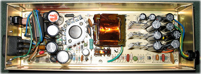
Apple II power supply

This is the AA11040-B power supply for the Apple II Plus.[59] AC power enters, on the left, is filtered, goes through the large switching transistor to the flyback transformer in the middle, is rectified by the diodes to the right (on heatsinks), and then is filtered by the capacitors on the right. The control circuitry is along the bottom. Photo used by permission from kjfloop, Copyright 2007.

The AC start mechanism was not used by the Apple II,[59] but was used by the Apple II Plus,[64] Apple III,[65] Lisa,[66] Macintosh,[67] and Mac 128K through Classic.[68] I could not find any non-Apple power supplies that use this mechanism,[69] except for a 1978 TV power supply,[70] and it became obsoleted by IC controllers, so this mechanism seems to have had no impact on computer power supply design.

The second mechanism in Holt's patent, the clamp winding and diode to return power in a flyback converter, was used in a variety of power supplies until the mid-1980s and then disappeared. Some examples are the Boschert OL25 power supply (1978),[60] Apple III (1980),[65] Apple's power supply documentation (1982),[59] Tandy hard drive (1982),[71] Tandy 2000 (1983),[72][73] Apple Lisa (1983),[66] Apple Macintosh (1984),[67] Commodore Model B128 (1984),[74] Tandy 6000 (1985),[75] and Mac Plus (1986) to Mac Classic (1990).[68] This flyback clamp winding seems to have been popular with Motorola in the 1980s, appearing in the MC34060 controller IC datasheet,[76] a 1983 designer's guide[77] (where the winding was described as common but optional), and a 1984 application note.[78]

Is this flyback clamp winding the innovation of Holt's that other companies ripped off? I thought so, until I found a 1976 power supply book that described this winding in detail,[35] which ruined my narrative. (Also note that forward converters (as opposed to flyback converters) had used this clamp winding dating back to 1956,[79][80][81] so applying it to a flyback converter doesn't seem like a huge leap in any case.)

One puzzling aspect of power supply discussion in the book Steve Jobs[1] is the statement that the Apple II's power supply is "like those used in oscilloscopes", since oscilloscopes are just one small use for switching power supplies. This statement apparently arose because Holt had previously designed a switching power supply for oscilloscopes,[82] but there's no other connection between Apple's power supply and oscilloscope power supplies.

The biggest impact of the Apple II on the power supply industry was on Astec - the Hong Kong company that manufactured the power supply. Before the Apple II came out, Astec was a little-known manufacturer, selling switching DC-DC inverters. But by 1982, Astec had become the world's top switching-powers-supply manufacturer, almost entirely based on Apple's business, and kept the top spot for a number of years.[83][84] In 1999, Astec was acquired by Emerson,[85] which is currently the second-largest power supply company after Delta Electronics.[86]

A little-known fact about the Apple II power supply is that it was originally assembled by middle-class California housewives as piecework.[83] As demand grew, however, power supply construction was transferred to Astec, even though it cost $7 a unit more. Astec was building 30,000 Apple power supplies monthly by 1983.[83]

Power supplies post-Apple

In 1981, the IBM PC was launched, which would have lasting impact on computer power supply designs. The power supply for the original IBM 5150 PC was produced by Astec and Zenith.[83] This 63.5W power supply used a flyback design controlled by a NE5560 power supply controller IC.[87]

I will compare the IBM 5150 PC power supply with the Apple II power supply in detail to show their commonalities and differences. They are both off-line flyback power supplies with multiple outputs, but that's about all they have in common. Even though the PC power supply uses an IC controller and the Apple II uses discrete components, the PC power supply uses approximately twice as many components as the Apple II power supply. While the Apple II power supply uses a variable frequency oscillator built out of transistors, the PC power supply uses a fixed-frequency PWM oscillator provided by the NE5560 controller IC. The PC uses optoisolators to provide voltage feedback to the controller, while the Apple II uses a small transformer. The Apple II drives the power transistor directly, while the PC uses a drive transformer. The PC checks all four power outputs against lower and upper voltage limits to make sure the power is good, and shuts down the controller if any voltages are out of spec. The Apple II instead uses a SCR crowbar across the 12V output if that voltage is too high. While the PC flyback transformer has a single primary winding, the Apple II uses an extra primary clamp winding to return power, as well as an another primary winding for feedback. The PC provides linear regulation on the 12V and -5V supplies, while the Apple II doesn't. The PC uses a fan, while the Apple II famously doesn't. It's clear that the IBM 5150 power supply does not "rip off" the Apple II power supply design, as they have almost nothing in common. And later power supply designs became even more different.

The IBM PC AT power supply became a de facto standard for computer power supplies. In 1995, Intel introduced the ATX motherboard specification,[88] and the ATX power supply (along with variants) has become the standard for desktop computer power supplies, with components and designs often targeted specifically at the ATX market.[89]

Computer power systems became more complicated with the introduction of the voltage regulator module (VRM) in 1995 for the Pentium Pro, which required lower voltage at higher current than the power supply could provide directly. To supply this power, Intel introduced the VRM - a DC-DC switching regulator installed next to the processor that reduces the 12 volts from the power supply to the low voltage used by the processor.[90] (If you overclock your computer, it is the VRM that lets you raise the voltage.) In addition, graphics cards can have their own VRM to power a high-performance graphics chip. A fast processor can require 130 watts from the VRM. Comparing this to the half watt of power used by the Apple II's 6502 processor[91] shows the huge growth in power consumption by modern processors. A modern processor chip alone can use more than twice the power of the whole IBM 5150 PC or three times that of the Apple II.

The amazing growth of the computer industry has caused the power consumption of computers to be a cause for environmental concern, resulting in initiatives and regulations to make power supplies more efficient.[92] In the US, Energy Star and 80 PLUS certification[93] pushes manufacturers to manufacture more efficient "green" power supplies. These power supplies squeeze out more efficiency through a variety of techniques: more efficient standby power, more efficient startup circuits, resonant circuits (also known as soft-switching and ZCT or ZVT) that reduce power losses in the switching transistors by ensuring that no power is flowing through them when they turn off, and "active clamp" circuits to replace switching diodes with more efficient transistor circuits.[94] Improvements in MOSFET transistor and high-voltage silicon rectifier technology in the past decade has also led to efficiency improvements.[92]

Power supplies can use the AC line power more efficiently through the technique of power factor correction (PFC).[95] Active power factor correction adds another switching circuit in front of the main power supply circuit. A special PFC controller IC switches this at a frequency of up to 250kHZ, carefully extracting a smooth amount of power from the power supply to produce high-voltage DC, which is then fed into a regular switching power supply circuit.[13][96] PFC also illustrates how power supplies have turned into a commodity with razor-thin margins, where a dollar is a lot of money. Active power factor correction is considered a feature of high-end power supplies, but its actual cost is only about $1.50.[97]

Many different controller chips, designs, and topologies have been used for IBM PC power supplies over the years, both to support different power levels, and to take advantage of new technologies.[98] Controller chips such as the NE5560 and SG3524 were popular in early IBM PCs.[99] The TL494 chip became very popular in a half-bridge configuration,[99] the most popular design in the 1990s.[100] The UC3842 series was also popular for forward converter configurations.[99] The push for higher efficiency has made double forward converters more popular,[101] and power factor correction (PFC) has made the CM6800 controller very popular,[102] since the one chip controls both circuits. Recently, forward converters that generate only 12V have become more common, using DC-DC converters to produce very stable 3.3V and 5V outputs.[94] More detailed information on modern power supplies is available from many sources.[103][104][98][105]
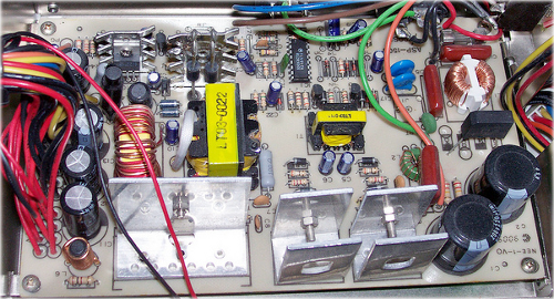
XT power supply

This typical 150W XT power supply uses the popular half-bridge design. The AC input filtering is on the right. To the left of this is the control/driver ciruit: the TL494 IC at the top controls the small yellow drive transfomer below, which drives the two switching transistors on the heatsinks below. To the left of this is the larger yellow main transformer, with the secondary diodes and regulator on the heatsinks, and output filtering to the left. This half-bridge power supply design is totally different from the Apple II's flyback design. Photo copyright larrymoencurly, used with permission.

Modern computers contain a surprising collection of switching power supplies and regulators. A modern power supply can contain a switching PFC circuit, a switching flyback power supply for standby power, a switching forward converter to generate 12 volts, a switching DC-DC converter to generate 5 volts, and a switching DC-DC converter to generate 3.3 volts,[94] so the ATX power supply can be considered five different switching power supplies in one box. In addition, the motherboard has a switching VRM regulator to power the processor, and the graphics card has another VRM, for a total of seven switching supplies in a typical desktop computer.

The technology of switching power supplies continues to advance. One development is digital control and digital power management.[106] Instead of using analog control circuits, digital controller chips digitize the control inputs and use software algorithms to control the outputs. Thus, designing the power supply controller becomes as much a matter of programming as of hardware design. Digital power management lets power supplies communicate with the rest of the system for higher efficiency and logging. While these digital technologies are largely used for servers now, I expect they will trickle down to desktop computers eventually.

To summarize, the original IBM 5150 PC power supply was different in almost every way from the Apple II power supply, except both were flyback power supplies. More recent power supplies don't even have that in common with the Apple II. It's absurd to claim that power supplies are ripping off Apple's design.

Famous switching power supply designers

Steve Jobs said that Rod Holt should be better known for designing the Apple II's power supply: "Rod doesn't get a lot of credit for this in the history books but he should."[1] But even at best, power supply designers aren't famous outside a very small community. Robert Boschert was inducted into Electronic Design's Electronic Engineering Hall of Fame in 2009 for his power supply work.[51] Robert Mammano got Power Electronics Technology's lifetime achievement award in 2005 for starting the PWM controller IC industry.[10] Rudy Severns got Power Electronics Technology's lifetime achievement award in 2008 for his innovations in switching power supplies.[107] But none of these people are even Wikipedia-famous. Other major innovators in the field get even less attention.[108] I repeatedly came across the work of Elliot Josephson, who designed satellite power systems in the early 1960s[18], has a bunch of power supply patents including the Tandy 6000[75], and even has his patent number printed on the Apple II Plus and Osborne 1 power supply circuit boards[59], but he appears to be entirely unrecognized.

The irony in Steve Jobs' comment that Rod Holt doesn't get a lot of credit is that Rod Holt's work is described in dozens of books and articles about Apple, from Revenge of the Nerds in 1982[109] to 2011's best-selling Steve Jobs biography, which makes Rod Holt easily the most famous power supply designer ever.

Conclusion

Power supplies aren't the boring metal boxes that most people think; they have a lot of interesting history, driven largely by the improvements in transistors that made switching power supplies practical for computers in the early 1970s. More recently, efficiency standards such as 80 PLUS have forced power supplies to become more efficient, resulting in new designs. The Apple II sold a huge number of switching power supplies, but its power supply design was a technological dead end that was not "ripped off" by other computers.

If you're interested in power supplies, you might also like my article Tiny, cheap, and dangerous: Inside a (fake) iPhone charger.

Notes and references

I spent way too much time researching power supplies, analyzing schematics and digging through old electronics journals. Here are my notes and references, in case they are of use to someone else. I'd be interested in hearing from power supply designers who have first-hand experience with the development of power supplies in the 1970s and 1980s.

[1] Steve Jobs, Walter Isaacson, 2011. Rod Holt's power supply design for the Apple II is discussed on page 74. Note that the description of a switching power supply in this book is rather garbled.

[2] PWM: From a Single Chip To a Giant Industry, Gene Heftman, Power Electronics Technology, pp48-53, Oct 2005.

[3] Preliminary Site Planning: Cray-1 Computer (1975) The Cray-1 used two 200 HP (150KW) motor-generator units to convert 250A 460V input AC into regulated 208V, 400Hz power; each motor-generator was approximately 3900 pounds. The 208V 400Hz power was fed into 36 separate power supplies that used twelve-phase transformers but no internal regulators. These power supplies famously formed the 12 benches around the Cray computer. Photographs of the Cray power components are in Cray-1 S Series Hardware Reference Manual (1981). This high-frequency motor-generator setup may seem strange, but the IBM 370 used a similar setup, see Announcing: IBM System/370 Model 145.

[4] Many larger computers used ferroresonant transformers for regulation. For instance, the power supply for the IBM 1401 computer used a 1250W ferroresonant regulator, see Reference Manual, 1401 Data Processing System (1961), p13. The HP 3000 Series 64/68/70 also used ferroresonant transformers, see Series 64/68/70 Computer Installation Manual (1986), p2-3. DEC used ferroresonant and linear power supplies almost exclusively in the early 1970s, including for the PDP-8/A (picture in "Power-supply choice looms large in sophisticated designs", Electronics, Oct 1976, volume 49, p111).

[5] "Power Supplies for Computers and Peripherals", Computer Design, July 1972, pp 55-65. This long article on power supplies has a lot of discussion of switching power supplies. It describes the buck (series), boost (shunt), push-pull (inverter), and full bridge topologies. The article says that the voltage rating of the switching transistor is the limiting parameter in many applications, but "high voltage, high speed transistors are increasingly available at low cost - and important factor in the more widespread use of switching regulator supplies." It concludes that "Availability of high voltage, high power, switching transistors at moderate prices is providing extra impetus to the use of high efficiency switching regular [sic] supplies. Substantial increase in usage is expected this year."

The article also says, "One of the more controversial topics is the continuing debate on the value of switching type supplies for computer applications, as contrasted with conventional series transistor regulators." This is echoed by some of the vendor comments. One skeptic was Elexon Power Systems, which "does not regard switching regulators as 'the answer.' They plan to disclose an entirely new power supply approach in the near future." Another was Modular Power Inc, who "recommend against switching regulators except when small size, light weight, and high efficiency are primary considerations, as in portable and airborne equipment." Sola Basic Industries said "their engineers are highly skeptical of the long term reliability of switching regulators in practical mass production designs, and predict transistor failure problems."

The "vendor comments" section of the article provides insight into the technology of the power supply industry in 1972: Hewlett Packard "specifies that a major influence today is the ready availability of high speed, high current, low cost transistors accelerated by the current trend toward switching type regulators. The company makes extensive use of switching in a full range of high power designs." Lambda Electronics "makes extensive use of switching regulators for outputs above about 100 W" which are designed to avoid fan cooling. Analog Devices offered precision supplies that use switching techniques for high efficiency. RO Associates "considers growth of switching power supplies to be a major change in the power supply design area". They offered miniature 20-kHz supplies, and low cost 60-kHz supplies. Sola Basic Industries "predict that minicomputer manufacturers will be using more transformerless switching regulators in 1972, for high efficiency and reduced size and weight." Trio Laboratories "indicates that computer and peripheral manufacturers are turning to switching types because pricing is now more competitive and applications are requiring reduced size."

[6] Practical switching power supply design, Marty Brown, 1990, p17.

[7] See the comment section for a detailed discussion of linear power supply efficiency.

[8] Power Supply Cookbook, Marty Brown, 2001. Page 5 discusses the relative development time for different power supply technologies, with a linear regulator taking 1 week of total development time, while a PWM switching regulator takes 8 person-months.

[9] A summary of different topologies is in SMPS overview and Power Supply Topologies. Details are in Microchip AN 1114: SMPS Topologies and Topologies for switched mode power supplies

[10] Lifetime Achievement Award Recipient Robert Mammano, Power Electronics Technology, Sep 2005, pp 48-51. This article describes the Silicon General SG1524 (1975) as the IC that ushered in the age of switching regulators and switch-mode power supplies.

[11] IBM Customer Engineering Reference Manual: 736 Power Supply, 741 Power Supply, 746 Power Distribution Unit (1958), page 60-17. The power supply for the 704 computer consists of three refrigerator-sized cabinets full of vacuum tubes, fuses, relays, mechanical timers, and transformers, using 90.8KVA of power. It used multiple regulation techniques including saturable-reactor transformers and thermistor-based reference voltage. The DC outputs were regulated by a 60 Hz thyratron switching mechanism. Thyratrons are switching vacuum tubes that control the output voltage (much like TRIACs in a common dimmer switch). This can be considered a switching power supply (see Power supplies, switching regulators, inverters, and converters, Irving Gottlieb, pp 186-188).

[12] In their ads, Pioneer Magnetics claims to have designed their first switching power supply in 1958. For instance, see Electronic Design, V27, p216.

[13] Unity power factor power supply, patent 4677366. Pioneer Magnetics filed this patent in 1986 on active power factor correction. See also Pioneer Magnetics' Why PFC? page.

[14] An early switching power supply was described in "A Transistor Power Converter-Amplifier", D. A. Paynter, General Electric Co., Solid-State Circuits Conference, 1959, p90-91. Also see related 1960 patent 3067378, Transistor Converter.

[15] Nondissipative DC to DC Regulator Converter Study, Goddard Space Flight Center, 1964. This survey of transistorized DC-DC converters shows about 20 different switching designs known in the early 1960s. The flyback converter is notably absent. Many other NASA reports on power converters from this time period are available from NASA Technical Reports Server.

[16] A detailed history of switching power supplies appears in S.J. Watkins' M.Phil. thesis Automatic testing of switched-mode power supplies, in the chapter History and Development of Switched-Mode Power Supplies Pre 1987.

[17] Switching Power Supply Development History, TDK Power Electronics World. This provides a very brief history of switching power supplies. TDK also has a surprisingly detailed discussion of switching power supplies in comic form: TDK Power Electronics World.

[18] "Satellite power supply has variable pulse width", Electronics, Feb 1962, p47-49. This article by Elliot Josephson of Lockheed describes a constant-frequency PWM DC-DC converter for satellites. See also patent 3219907 Power Conversion Device.

[19] The Spacecraft Power Supply System, Telstar, 1963. The Telstar satellite obtained power from solar cells, storing the power in NiCad batteries. Efficiency was critical for the satellite, so a DC-to-DC switching voltage regulator was used, with a buck converter converting the variable battery voltage into stable -16 V DC at up to 32 watts at up to 92% efficiency. Because the satellite needed a wide range of voltages, up to 1770 volts for the RF amplifier, additional converters were used. The regulated DC was inverted to AC, fed into transformers, and rectified, to produce the required voltages.

[20] Some PDP models, such as the PDP-11/20 used the H720 power supply (see PDP handbook, 1969). This power supply is described in detail in H720 Power Supply and Mounting Box Manual (1970). The 25 pound power supply uses a power transformer to generate 25V DC, and then switching switching regulators (buck converter) to generate 230W of regulated +5 and -15 volts. Because transistors of the era couldn't handle high voltages, the DC voltage had to be reduced to 25 volts by a large power transformer.

[21] "The Switching Regulator Power Supply", Electronics World v86 October 1971, p43-47. This long article on switching power supplies was featured on the cover of Electronics World. The article is worth looking up, if only for the picture of the F-111 aircraft's switching power supply, which looks so complex that I'd almost expect it to land the plane. The switching power supplies discussed in this article combine a switching DC-DC inverter with a transformer for isolation with a separate buck or boost switching regulator. As a result, the article claims that switching power supplies will always be more expensive than linear power supplies because of the two stages. Modern power supplies, however, combine both stages. The article discusses a variety of power supplies including the 250W switching power supply used by the Honeywell H316R. The article says that the switching regulator power supply had come of age because of new advances in high-speed and high-power transistors. The cover shows a 500W switching power supply that according to the article could not have been built with the transistors available just a year and a half earlier.

[22] A Bantam Power Supply for a Minicomputer, Hewlett-Packard Journal, October 1971. Circuit details in High Efficiency Power Supply patent 3,852,655. This is a 492W off-line power supply using inverters followed by 20V switching regulators.

[23] The HP2100A was introduced in 1971 with a switching power supply (see HP2100A Main Specifications). It is claimed to have the first switching power supply in a minicomputer 25 Years of Real-Time Computing, but the PDP-11/20 was earlier.

[24] A Computer Power System for Severe Operating Conditions, p21, Hewlett-Packard Journal, Oct 1974. The 21MX minicomputer used a 300 W, off-line, switching preregulator to generate regulated 160V DC which was fed into switching dc-to-dc converters.

[25] Data General Technical Manual Nova 2, 1974. The Nova 2/4 used switching regulator to generate 5V and 15V, while the larger 2/10 used a constant voltage transformer. The manual says, "At the higher current losses associated with a computer, the losses [from linear regulators] may become excessive, and for this reason the switching regulator is often used, as in the NOVA 2/4."

[26] Model 960B/980B Computer Maintenance Model: Power Supply The power supply for the Texas Instruments 960B minicomputer used a switching regulator for the 150W 5V supply and linear regulators for the other voltages. The switching regulator consists of two parallel buck converters running at 60kHz, and using 2N5302 NPN switching transistors (introduced in 1969). Because the transistors have a 60V maximum rating, the power supply uses a transformer to drop the voltage to 35V that is fed into the regulator.

[27] M49-024 and M49-026 Switching Regulated Power Supply Instruction Manual, Interdata, 1974. These off-line half-bridge power supplies provided 120W or 250W and were used by the Interdata minicomputers. The switching oscillator used 555 and 556 timer chips.

[28] 2640A Power Supply, Hewlett-Packard Journal, June 1975, p 15. "A switching mode power supply was chosen because of the efficiency and space requirement." Also Data Terminal Technical Information. Another point of interest is its case molded of structural foam (p23) which is very similar to the Apple II's foam-molded plastic case (see page 73 of Steve Jobs), and a couple years earlier.

[29] "Power-supply choice looms large in sophisticated designs", Electronics, Oct 1976, volume 49. p107-114. This long article discusses power supplies including switching power supplies in detail. Note that the Selectric Composer is very different from the popular Selectric typewriter.

[30] IBM 5100 Portable Computer Maintenance Information Manual. The IBM 5100 was a 50-pound portable computer that used BASIC and APL, and included a monitor and tape drive. The power supply is described on page 4-61 as a small, high power, high frequency transistor switching regulator supply that provides 5V, -5V, 8.5V, 12V, and -12V.

[31] The HP 9825A Desktop Computer from 1976 used a switching regulator for the 5V power supply. It also used a foam-molded case, predating the Apple II's; see 98925A Product Design, Hewlett-Packard Journal, June 1976, p5.

[32] Mid-Range Calculator Delivers More Power at Lower Cost, Hewlett-Packard Journal, June 1976 discusses the 5V switching power supply used by the 9815A calculator.

[33] DEC's H7420 power supply is described in decsystem 20 Power Supply System Description (1976). It holds 5 switching regulators to provide multiple voltages, and provides about 700 W. The power supply uses a large transformer to reduce the line voltage to 25V DC, which is passed to the individual switching regulators, which use a buck topology to obtain the desired voltage (+5, -5, +15, or +20).

The decsystem 20 minicomputer was a large system, consisting of three refrigerator-sized cabinets. It took a hefty 21.6 KW of three-phase input power, which is regulated by a combination of switching and linear regulators. It contained seven H7420 power supplies and about 33 individual switching regulator units, as well as a linear regulator for the CPU that used -12V DC at 490A.

[34] Switching power supplies for television receivers seemed to gain momentum around 1975-1976. Philips introduced the TDA2640 for television switched-mode power supplies in 1975. Philips published a book, Switched-mode power supplies in TV receivers in 1976. One drawback of the increasing use of switched-mode power supplies in TVs was they caused interference with amateur radio, as discussed by Wireless World, v82, p52, 1976.

[35] "Electronic Power Control and Digital Techniques", Texas Instruments, 1976. This book discusses switching power supplies in detail.

Chapter IV "Inverter/Converter Systems" describes a simple 120W flyback power supply using a SCR-driven BUY70B power transistor. Of note, this circuit uses an additional primary winding with diode to return unused energy to the source.

Chapter V "Switching Mode Power Supplies" describes the construction of a 5V 800W switching power supply based on an off-line switching shunt regulator followed by a DC-DC converter. It also describes a fairly simple multiple-output flyback power supply controlled by a SN76549, designed for a large screen color television.

[36] Power Electronics Milestones, Power Sources Manufacturers Association.

[37] In 1967 RO Associates introduced the first successful switching power supply product, the 20-kHz, 50-W switching power supply, the Model 210. (See "RO first into switching supplies", Electronic Business, Volume 9, 1983, p36.) They claimed to be the leaders in switching power supplies by 1976. Their 1969 patent 3564384 "High Efficiency Power Supply Apparatus" describes a half-bridge switching power supply that is surprisingly similar to the ATX power supplies popular in the 1990s, except mag amp circuits controlled the PWM rather than the ubiquitous TL494 controller IC.

[38] Nippon Electronic Memory Industry Co (NEMIC, which ended up part of TDK-Lambda) started developing standardized switching power supplies in 1970. History of TDK-Lambda Corporation.

[39] "I forecast that the majority of companies, after several false starts in the power-supplies field will be offering, by the end of 1972, ranges of switching power supplies with acceptable specifications and RFI limits.", page 46, Electronic Engineering, Volume 44, 1972.

[40] Power supply manufacturer Coutant built a power supply called the Minic using "a relatively new switching regulator technique". Instrument practice for process control and automation, Volume 25, p471, 1971.

[41] "Switching power supplies reach the marketplace", p71, Electronics & Power, February 1972. The first "transformerless" switching power supply reached the UK market in 1972, APT's SSU1050, which was an adjustable 500W switching power supply using a half-bridge topology. This 70-pound power supply was considered lightweight compared to linear power supplies.

[42] This article explains switching power supplies in depth, describing the advantages of off-line power supplies. It describes the half-bridge MG5-20 miniature switching power supply built by Advance Electronics. The article says, "The widespread application of microelectronic devices accentuated the sheer bulk of conventional power supplies. Switching converters have now become viable and offer appreciable savings in volume and weight." "Switching power supplies: why and how", Malcolm Burchall, Technical Director,Power Supplies Division, Advance Electronics Ltd. Electronic Engineering, Volume 45, Sept 1973, p73-75.

[43] High-Efficiency Modular Power Supplies Using Switching Regulators, Hewlett-Packard Journal, December 1973, p 15-20. The 62600 series provides 300W using an off-line, half-bridge topology switching power supply. The key was the introduction of 400V, 5A transistors with sub-microsecond switching times. "A complete 300 W switching regulated supply is scarcely larger than just the power transformer of an equivalent series-regulated supply, and it weighs less - 14.5 lbs vs the transformer's 18 lbs."

[44] A High-Current Power Supply for Systems That Use 5 Volt IC Logic Extensively, Hewlett-Packard Journal, April 1975, p 14-19. The 62605M 500W switching power supply for OEMs at 1/3 the size and 1/5 the weight of linear supplies. Uses an off-line half bridge topology.

[45] Modular Power Supplies: Models 63005C and 63315D: This 110W 5V power supply used an off-line forward converter topology, and was convection cooled without a fan.

[46] "The penetration of switching supplies in the US power-supply market will grow from 8% in 1975 to 19% by 1980. This increasing penetration corresponds to the worldwide trend and represents a very high growth rate." Several reasons were given for this predicted growth, including "the availability of better components, reduced overall cost, [...] and the advent of smaller products (such as microcomputers) that make smaller power units desirable." Electronics, Volume 49. 1976. Page 112, sidebar "What of the future?"

[47] Seymour Levine, "Switching Power Supply Regulators For Greater Efficiency." Electronic Design, June 22. 1964. This article describes how switching regulators can increase efficiency from less than 40 percent to more than 90 percent with substantial savings in size, weight, and cost.

[48] The cover of Electronic Design 13, June 21, 1976 says, "Suddenly it's easier to switch. Switching power supplies can be designed with 20 to 50 fewer discrete components than before. A single IC performs all of the control functions required for a push-pull output design. The IC is called a regulating pulse-width modulator. To see if you would rather switch, turn to page 125." Page 125 has an article, "Control a switching power supply with a single LSI circuit" that describes the SG1524 and TL497 switching power supply ICs.

[49] In 1976, Powertec was running two-page ads describing the advantages of switching power supplies, titled "The big switch is to switchers". These ads described the benefits of the power supplies: with twice the efficiency, they gave off 1/9 the heat. They had 1/4 the size and weight. The provided improved reliability, worked under brownout conditions, and could handle much longer power interruptions. Powertec sold a line of switching power supplies up to 800W. They suggested switching power supplies for add-on memory systems, computer mainframes, telephone systems, display consoles, desktop instruments, and data acquisition systems. Pages 130-131, Electronics v49, 1976.

[50] Byte magazine, p100 June 1976 announced the new Boschert OL80 switching power supply providing 80 watts in a two-pound power supply, compared to 16 pounds for a less-powerful linear power supply. It was also advertised in Microcomputer Digest, Feb 1976, p12.

[51] Robert Boschert: A Man Of Many Hats Changes The World Of Power Supplies: he started selling switching power supplies in 1974, focusing on making switching power supplies simple and low cost. The heading claims "Robert Boschert invented the switching power supply", which must be an error by the editor. The article more reasonably claims Boschert invented low-cost, volume-usage switching-mode power supplies. He produced a low-cost switching power supply in volume in 1974.

[52] The Diablo Systems HyTerm Communications Terminal Model 1610/1620 Maintenance Manual shows a 1976 Boschert push-pull power supply and a 1979 LH Research half-bridge power supply.

[53] Boschert's F-14 and satellite experience was touted in ads in Electronic Design, V25, 1977, which also mentioned volume production for Diablo and Qume.

[54] An unusual switching power supply was used by the HP 1000 A600 computer (see Engineering and Reference Documentation) (1983). The 440W power supply provided standard 5V, 12V, and -12V outputs, but also a 25kHz 39V AC output which was used to distribute power to other cards within the system, where it was regulated. The Boschert-designed off-line push-pull power supply used a custom HP IC, somewhat like a TL494.

[55] Multiple 450v switching transistor product lines were introduced in 1971 to support off-line switching power supplies, such as the SVT450 series, the 40850 to 4085 from RCA, and the 700V SVT7000 series.

[56] PWM: From a Single Chip To a Giant Industry, Power Electronics Technology, Oct 2005. This article describes the history of the power supply control IC, from the SG1524 in 1975 to a multi-billion dollar industry.

[57] "The revolution in power supply design now under way will not be complete until the 60-Hz transformer has been almost entirely replaced.", Walter Hirschberg, ACDC Electronics Inc, CA. "New components spark power supply revolution", p49, Canadian Electronics Engineering, v 17, 1973.

[58] Switching and linear power supply, power converter design, Pressman 1977 "Switching regulators - which are in the process of revolutionizing the power supply industry because of their low internal losses, small size, and weight and costs competitive with conventional series-pass or linear power supplies."

[59] Multiple Apple power supplies are documented in Apple Products Information Pkg: Astec Power Supplies (1982). The Apple II Astec AA11040 power supply is a simple discrete-component flyback power supply with multiple outputs. It uses a 2SC1358 switching transistor. The 5V output is compared against a Zener diode and control feedback and isolated through a transformer with two primary windings and one secondary. It uses the flyback diode clamp winding.

The AA11040-B (1980) has substantial modifications to the feedback and control circuitry. It uses a 2SC1875 switching transistor and a TL431 voltage reference. The AA11040-B was apparently used for the Apple II+ and Apple IIe (see hardwaresecrets.com forum). The silk screen on the power supply PCB says it is covered by patent 4323961, which turns out to be "Free-running flyback DC power supply" by Elliot Josephson and assigned to Astec. The schematic in this patent is basically a slightly simplified AA11040-B. The feedback isolation transformer has one primary and two secondary windings, the reverse of the AA11040. This patent is also printed on the Osborne 1 power supply board (see Osborne 1 teardown), which also uses the 2SC1875.

The Apple III Astec AA11190 uses the flyback diode clamp winding, but not Holt AC startup circuit. It uses a 2SC1358 switching transistor; the feedback / control circuitry is very similar to the AA11040-B. The Apple III Profile disk drive power supply AA11770 used the flyback diode clamp winding, a 2SC1875 switching transistor; again, the feedback / control circuitry is very similar to the AA11040-B. The AA11771 is similar, but adds another TL431 for the AC ON output.

Interestingly in this document Apple reprints ten pages of HP's "DC Power Supply Handbook" (1978 version used by Apple) to provide background on switching power supplies.

[60] Flyback converters: solid-state solution to low-cost switching power supply, Electronics, Dec 1978. This article by Robert Boschert describes the Boschert OL25 power supply, which is a very simple discrete-component 25W flyback power supply providing 4 outputs. It includes the flyback diode clamp winding. It uses a TL430 voltage reference and optoisolator for feedback from the 5V output. It uses a MJE13004 switching transistor.

[61] The Macintosh Performa 6320 used the AS3842 SMPS controller IC, as can be seen in this picture. The AS3842 is Astec's version of the UC3842 current-mode controller, which was very popular for forward converters.

[62] Power supply details for the iMac are difficult to find, and there are different power supplies in use, but from piecing together various sources, the iMac G5 appears to use the TDA4863 PFC controller, five 20N60C3 MOS power transistors, SG3845 PWM controller, TL431 voltage references, and power supervision by a WT7515 and LM339. A TOP245 5-pin integrated switcher is also used, probably for the standby power.

[63] DC Power Supply, #4130862 which was filed in February 1978 and issued in December 1978. The power supply in the patent has some significant differences from the Apple II power supply built by Astec. Much of the control logic is on the primary side in the patent and the secondary side in the actual power supply. Also, the feedback coupling is optical in the patent and uses a transformer in the power supply. The Apple II power supply doesn't use the AC feedback described in the patent.

[64] A detailed discussion of the Apple II Plus power supply is at applefritter.com. The description erroneously calls the power supply a forward converter topology, but it is a flyback topology. Inconveniently, this discussion doesn't match the Apple II Plus power supply schematics I've found. Notable differences: the schematic uses a transformer to provide feedback, while the discussion uses an optoisolator. Also, the power supply in the discussion uses the AC input to start the transistor oscillation, while the schematic does not.

[65] Apple III (1982). This Apple III power supply (050-0057-A) is almost totally different from the Apple III AA11190 power supply. This is a discrete-component flyback power supply with an MJ8503 switching transistor driven by a SCR, the flyback clamp winding, and 4 outputs. It uses the Holt AC startup circuit. The switching feedback monitors the -5V output with a 741 op amp and is connected via a transformer. It uses a linear regulator on the -5V output.

[66] Apple Lisa (1983). Another discrete-component flyback power supply, but considerably more complex than the Apple II, with features such as standby power, remote turn-on via a triac, and a +33V output. It uses a MJ8505 NPN power transistor driven by a SCR for switching. It uses the Holt AC startup circuit. The switching feedback monitors the +5V sense (compared to the linearly-regulated -5V output) and is connected via a transformer.

[67] Macintosh power supply. This flyback power supply uses the diode clamp winding and the Holt AC startup circuit. It uses a 2SC2335 switching transistor controlled by a discrete oscillator. The switching feedback monitors the +12V output using Zener diodes and a LM324 op amp and is connected through an optoisolator.

[68] Mac 128K schematic, Mac Plus discussion. This flyback power supply uses the diode clamp winding and Holt AC startup circuit. It uses a 2SC2810 switching transistor controlled by discrete components. The switching feedback monitors the 12V output and is connected via an optoisolator. Interestingly, this document claims that the power supply was notoriously prone to failure because it didn't use a fan. The Mac Classic power supply appears to be identical.

[69] TEAM ST-230WHF 230 watt switch mode power supply. This schematic is the only non-Apple computer power supply I have found that feeds raw AC into the drive circuit (see R2), but I'm sure this is just a drawing error. R2 should connect to the output of the diode bridge, not the input. Compare with R3 in an almost-identical drive circuit in this ATX power supply.

[70] Microprocessors and Microcomputers and Switching Mode Power Supplies, Bryan Norris, Texas Instruments, McGraw-Hill Company, 1978. This book describes switching power supplies for televisions that use the AC signal to start oscillation.

[71] Tandy hard drive power supply (Astec AA11101) . This 180W flyback power supply uses the diode clamp winding. It uses a 2SC1325A switching transistor. The oscillator uses discrete components. Feedback from the 5V rail is compared against a TL431 voltage reference, and feedback uses a transformer for isolation.

[72] Tandy 2000 power supply (1983). This 95W flyback power supply uses the MC34060 controller IC, a MJE12005 switching transistor, and has the flyback clamp winding. It uses a MC3425 to monitor the voltage, has a linear regulator for the -12V output, and provides feedback based on the 5V output compared with a TL431 reference, feed through an optoisolator. The 12V output uses a mag amp regulator.

[73] The Art of Electronics has a detailed discussion of the Tandy 2000 power supply (p 362).

[74] Commodore Model B128. This flyback power supply uses the diode clamp winding. It uses a MJE8501 switching transistor controlled by discrete components, and the switching feedback monitors the 5V output using a TL430 reference and an isolation transformer. The 12V and -12V outputs use linear regulators.

[75] Tandy 6000 (Astec AA11082). This 140W flyback power supply uses the diode clamp winding. The circuit is a rather complex discrete circuit, since it uses a boost circuit described in Astec patent 4326244, also by Elliot Josephson. It uses a 2SC1325A switching transistor. It has a slightly unusual 24V output. One 12V output is linearly regulated by a LM317, and the -12V output controlled by a a MC7912 linear regulator, but the other 12V output does not have additional regulation. Feedback is from the 5V output, using a TL431 voltage source and an isolation transformer. There's a nice photo of the power supply here.

[76] MC34060 controller IC (1982) documentation.

[77] The Designer's Guide for Switching Power Supply Circuits and Components, The Switchmode Guide, Motorola Semiconductors Inc., Pub. No. SG79, 1983. R J. Haver. For the flyback converter, the clamp winding is described as optional, but "usually present to allow energy stored in the leakage reactance to return safely to the line instead of avalanching the switching transistor."

[78] "Insuring Reliable Performance from Power MOSFETs", Motorola application note 929, (1984) shows a flyback power supply using the MC34060 with the clamp winding and diode. This can be downloaded from datasheets.org.uk.

[79] For more information on forward converters, see The History of the Forward Converter, Switching Power Magazine, vol.1, no.1, pp. 20-22, Jul. 2000.

[80] An early switching converter with an diode clamp winding was patented in 1956 by Philips, patent 2,920,259 Direct Current Converter.

[81] Another patent showing an energy-return winding with diode is Hewlett-Packard's 1967 patent 3,313,998 Switching-regulator power supply having energy return circuit

[82] The Little Kingdom: The Private Story of Apple Computer, Michael Moritz, 1984 says that Holt had worked at a Midwest company for almost ten years and helped design a low-cost oscilloscope (p164). Steve Jobs, the Journey Is the Reward, Jeffrey Young, 1988, states that Holt had designed a switching power supply for an oscilloscope ten years before joining Apple (p118). Given the state of switching power supplies at the time, this is almost certainly an error.

[83] "Switching supplies grow in the bellies of computers", Electronic Business, volume 9, June 1983, p120-126. This article describes the business side of switching power supplies in detail. While Astec was the top switching power supply manufacturer, Lambda was the top AC-DC power supply manufacturer because it sold large amounts of both linear and switching power supplies.

[84] "Standards: A switch in time for supplies", Electronic Business Today, vol 11, p74, 1985. This article states that Astec is the world's leading merchant maker of power supplies and the leader in switching power supplies. Astec grew almost solely on supplying power supplies to Apple. This article also names the "big 5" power supply companies as ACDC, Astec, Boschert, Lambda, and Power One.

[85] Astec Becomes Wholly-Owned Subsidiary of Emerson Electric, Business Wire, April 7, 1999.

[86] An industry report on the top power supply companies as of 2011 is Power Electronics Industry News, v 189, March 2011, Micro-Tech Consultants. Also, Power-Supply Industry Continues March to Consolidation, Power Electronics Technology, May 2007 discusses various consolidations.

[87] The SAMS photofact documentation for the IBM 5150 provides a detailed schematic of the power supply.

[88] Wikipedia provides an overview of the ATX standard. The official ATX specification is at formfactors.org.

[89] ON Semiconductor has ATX power supply Reference Designs, as does Fairchild. Some ICs designed specifically for ATX applications are SG6105 Power Supply Supervisor + Regulator + PWM, NCP1910 High Performance Combo Controller for ATX Power Supplies, ISL6506 Multiple Linear Power Controller with ACPI Control Interfaces, and SPX1580 Ultra Low Dropout Voltage Regulator.

[90] Intel introduced the recommendation of a switching DC-DC converter next to the processor in Intel AP-523 Pentium Pro Processor Power Distribution Guidelines, which provides detailed specifications for a voltage regulator module (VRM). Details of a sample VRM are in Fueling the megaprocessor - A DC/DC converter design review featuring the UC3886 and UC3910. More recent VMR specifications are in Intel Voltage Regulator Module (VRM) and Enterprise Voltage Regulator-Down (EVRD) 11 Design Guidelines (2009).

[91] The R650X and R651X microprocessors datasheet specifies typical power dissipation of 500mW.

[92] Power Conversion Technologies for Computer, Networking, and Telecom Power Systems - Past, Present, and Future, M. M. Jovanovic, Delta Power Electronics Laboratory, International Power Conversion & Drive Conference (IPCDC) St. Petersburg, Russia, June 8-9, 2011.

[93] The 80 Plus program is explained at 80 PLUS Certified Power Supplies and Manufacturers, which describes the various levels of 80 PLUS: Bronze, Silver, Gold, Platinum, and Titanium. The base level requires efficiency of at least 80% under various loads, and the higher levels require increasingly high efficiencies. The first 80 PLUS power supplies came out in 2005.

[94] A few random examples of power supplies that first generate just 12V, and use DC-DC converters to generate 5V and 3.3V outputs from this: ON Semiconductor's High-Efficiency 255 W ATX Power Supply Reference Design (80 Plus Silver), NZXT HALE82 power supply review, SilverStone Nightjar power supply review.

[95] Power supplies only use part of the electricity fed through the power lines; this gives them a bad "power factor" which wastes energy and increases load on the lower lines. You might expect that this problem arises because switching power supplies turn on and off rapidly. However, the bad power factor actually comes from the initial AC-DC rectification, which uses only the peaks of the input AC voltage.

[96] Power Factor Correction (PFC) Basics, Application Note 42047, Fairchild Semiconductor, 2004.

[97] Right Sizing and Designing Efficient Power Supplies states that active PFC adds about $1.50 to the cost of a 400W power supply, active clamp adds 75 cents, and synchronous rectification adds 75 cents.

[98] Many sources of power supply schematics are available on the web. Some are andysm, danyk.wz.cz, and smps.us. A couple sites that provide downloads of power supply schematics are eserviceinfo.com and elektrotany.com.

[99] See the SMPS FAQ for information on typical PC power supply design. The sections "Bob's description" and "Steve's comments" discuss typical 200W PC power supplies, using a TL494 IC and half-bridge design.

[100] A 1991 thesis states that the TL494 was still used in the majority of PC switched mode power supplies (as of 1991). The development of a 100 KHZ switched-mode power supply (1991). Cape Technikon Theses & Dissertations. Paper 138.

[101] Introduction to a two-transistor forward topology for 80 PLUS efficient power supplies, EE Times, 2007.

[102] hardwaresecrets.com states that the CM6800 is the most popular PFC/PWM controller. It is a replacement for the ML4800 and ML4824. The CM6802 is a "greener" controller in the same family.

[103] Anatomy of Switching Power Supplies, Gabriel Torres, Hardware Secrets, 2006. This tutorial describes in great detail the operation and internals of PC power supplies, with copious pictures of real power supply internals. If you want to know exactly what each capacitor and transistor in a power supply does, read this article.

[104] ON Semiconductor's Inside the power supply presentation provides a detailed, somewhat mathematical guide to how modern power supplies work.

[105] SWITCHMODE Power Supply Reference Manual, ON Semiconductor. This manual includes a great deal of information on power supplies, topologies, and many sample implementations.

[106] Some links on digital power management are Designers debate merits of digital power management, EE Times, Dec 2006. Global Digital Power Management ICs Market to Reach $1.0 Billion by 2017. TI UCD9248 Digital PWM System Controller. Free ac/dc digital-power reference design has universal input and PFC, EDN, April 2009.

[107] Rudy Severns, Lifetime Achievement Award Winner, Power Electronics Technology, Sept 2008, p40-43.

[108] Where Have All the Gurus Gone?, Power Electronics Technology, 2007. This article discusses the contributions of many power supply innovators including Sol Gindoff, Dick Weise, Walt Hirschberg, Robert Okada, Robert Boschert, Steve Goldman, Allen Rosenstein, Wally Hersom, Phil Koetsch, Jag Chopra, Wally Hersom, Patrizio Vinciarelli, and Marty Schlecht.

[109] The story of Holt's development of the Apple II power supply first appeared in Paul Ciotti's article Revenge of the Nerds (unrelated to the movie) in California magazine, in 1982.

Tiny, cheap, and dangerous: Inside a (fake) iPhone charger

$
0
0

I recently wrote a popular article on the history of computer power supplies, which led to speculation on what's inside those amazingly small one-inch cube USB chargers sold by Apple, Samsung, RIM, and other companies. In the interest of science, I bought a cheap no-name cube charger off eBay for $2.79, and took it apart. It's amazing that manufacturers can build and sell a complex charger for just a few dollars. It looks a lot like a genuine Apple charger and cost a lot less. But looking inside, I found that important safety corners were cut, which could lead to a 340 volt surprise. In addition, the interference from a cheap charger like this can cause touchscreen malfunctions. Thus, I recommend spending a few dollars more to get a brand-name charger.
A one-inch USB charger designed for the iphone4
The no-name charger I bought is just over an inch in length, excluding the Eurpopean-style plug. The charger is labeled "FOR iphone4. Input 110-240V 50/60Hz Output 5.2V 1000mA, Made in China." There are no other markings (manufacturer, serial number, or safety certifications). I opened up the charger with a bit of Dremel-ing. One surprise is how much empty space is inside for a charger that's so small. Apparently the charger circuit is designed for a smaller US-style plug, and the extra space with a European plug is unused. Since the charger accepts 110 to 240V input, the same circuit can be used worldwide.[1]
Inside a USB phone charger
The power supply itself is slightly smaller than one cubic inch. The picture below shows the main components. On the left is the standard USB connector. Note how much room it takes up - it's not surprising devices are moving to micro-USB connectors. The flyback transformer is the black and yellow component; it converts the high-voltage input to the 5V output. In front of it is the switching transistor. Next to the transistor is a component that looks like a resistor but is an inductor filtering the AC input. On the underside, you can see the capacitors that filter the output and input.
Internals of a USB phone charger
The power supply is a simple flyback switching power supply. The input AC is converted to high-voltage DC by a diode, chopped into pulses by the power transistor and fed into the transformer. The transformer output is converted to low voltage DC by a diode, filtered, and fed out through the USB port. A feedback circuit regulates the output voltage at 5 volts by controlling the chopping frequency.

Detailed explanation

In more detail, the power supply is a self-oscillating flyback converter, also known as a ringing choke converter.[2] Unlike most flyback power supplies, which use a IC to control the oscillation, this power supply oscillates on its own through a feedback winding on the transformer. This reduces the component count and minimizes cost. A 75 cent controller IC[3] would be a huge expense for a $2.79 power supply, so they used a minimal circuit instead.
The circuit board inside a tiny USB charger
The above picture shows the circuit components; the red boxes and italics indicate components on the other side. (Click for a larger picture.) Note that most of the components are tiny surface-mounted devices (SMD) and are dwarfed by the capacitors. The green wires supply the input AC, which is filtered through the inductor. The high-voltage 1N4007 (M7) input diode and the 4.7µF input capacitor convert the AC input to 340 volts DC.[4] The MJE13003 power transistor switches the power to the transformer at a variable frequency (probably about 50kHz). The transformer has two primary windings (the power winding and a feedback winding), and a secondary winding. (The transformer and inductor are also known as "the magnetics".)

On the secondary (output) side, the high-speed SS14 Schottky diode rectifies the transformer output to DC, which is filtered by the 470µF output capacitor before providing the desired 5V to the USB port. The two center pins of the USB port (the data pins) are shorted together with a blob of solder, as will be explained below.

A simple feedback circuit regulates the voltage. The output voltage is divided in half by a resistor divider and compared against 2.5V by the common 431 voltage reference device. The feedback is passed to the primary side through the 817B optoisolator. On the primary side, the feedback oscillation from the feedback transformer winding and the voltage feedback from the optoisolator are combined in the 2SC2411 control transistor. This transistor then drives the power transistor, closing the loop. (A very similar power supply circuit is described by Delta.[5])

Isolation and safety

For safety reasons, AC power supplies must maintain strict isolation between the AC input and the output. The circuit is divided into a primary side - connected to AC, and a secondary side - connected to the output. There can be no direct electrical connection between the two sides, or else someone touching the output could get a shock. Any connection between the two sides must go through a transformer or optoisolator. In this power supply, the transformer provides isolation of the main power, and the optoisolator provides isolation of the feedback of the secondary voltage.

If you look at the picture, you can see the isolation boundary indicated as a white line on the circuit board crossing the circuit board roughly horizontally, with the primary side on top and the secondary side below. (This line is printed on the board; I didn't add it to the picture.) The circles on the line that look like holes are, in fact, holes. These provide additional isolation between the two sides.

The UL has complex safety specifications on how much distance (known as "creepage" and "clearance") there must be between the primary and secondary sides to prevent a shock hazard.[6] The rules are complicated and I'm no expert, but I think at least 3 or 4 mm is required. On this power supply, the average distance is about 1 millimeter. The clearance distance below R8 on the right is somewhat less than one millimeter (notice that white line crosses the PCB trace to the left of R8).

I wondered how this power supply could have met the UL standards with clearance less than 1 mm. Looking at the charger case more closely, I noticed that it didn't list any safety certifications, or even a manufacturer. I suddenly realized that purchasing the cheapest possible charger on eBay from an unknown manufacturer in China could actually be a safety hazard. Note that this sub-millimeter gap is all that's protecting you and your phone from potentially-lethal 340 volts. I also took the transformer apart and found only single layers of insulating tape between the windings, rather than the double layers required by the UL. After looking inside this charger, my recommendation is to spend a bit more on a charger, and get one that has UL approval and a name-brand manufacturer.

Another issue with super-cheap chargers is they produce poor-quality electrical output with a lot of noise that can interfere with the operation of your phone. Low-cost ringing choke adapters are known to cause touchscreen malfunctions because the screen picks up the electrical interference.[7] In noticed several cost-saving design decisions that will increase interference. The charger uses a single diode to rectify the input, rather than a four-diode bridge, which will produce more interference. The input and output filtering are minimal compared to other designs.[8][9] There's also no fuse on the AC input, which is a bit worrying.

USB charging protocols

You might think USB chargers are interchangeable and plugging a USB device into a charger is straightforward, but it turns out that it's a mess of multiple USB charging standards,[10][11][12] devices that break the rules,[13] and proprietary protocols used by Sony and Apple.[14][15][16] The underlying problem is that a standard USB port can provide up to 500mA, so how do chargers provide 1A or more for faster charging? To oversimplify, a charger indicates that it's a charger by shorting together the two middle USB pins (D+ and D-). Proprietary chargers instead connect different resistances to the D+ and D- pins to indicate how much current they can provide. Note that there are a few unused resistor spots (R2, R3, R8, R10) connected to the USB port on the circuit above; the manufacturer can add the appropriate resistors to emulate other types of chargers.

Advances in AC power adapters

Early power adapters were just an AC transformer producing low-voltage AC, or add diodes to produce DC. In the mid 1990s, switching power supplies became more popular, because they are more compact and more efficient.[17] However, the growing popularity of AC adapters along with their tendency to waste a few watts when left plugged in ended up costing the United States billions of dollars in wasted electricity every year.[3] New Energy Star standards[18] encouraged "green" designs that use milliwatts rather than watts of power when idle. These efficient controllers can stop switching when unloaded, with intermittent bursts to get just enough power to keep running.[19] One power supply design actually achieves zero standby power usage, by running off a "supercapacitor" while idle.[20]

The semiconductor industry continues to improve switching power supplies through advances in controller ICs and switching transistors. For simple power supplies, some manufacturers combine the controller IC and the switching transistor into a single component with only 4 or 5 pins. Another technology for charger control is CC/CV, which provides constant current until the battery is charged and then constant voltage to keep it charged. To minimize electromagnetic interference (EMI), some controllers continuously vary the switching frequency to spread out the interference across a "spread spectrum".[21] Controllers can also include safety features such as overload protection, under voltage lockout, and thermal shutdown to protect against overheating,

Conclusions

Stay away from super-cheap AC adapters built by mystery manufacturers. Spend the extra few dollars to get a brand-name AC adapter. It will be safer, produce less interference, and your device's touchscreen will perform better.
Inside a inch cube cellphone charger

Notes and references

[1] Switching power supplies often take a "universal" input of 110V to 240V at 50/60 Hz, which allows the same supply to conveniently work on worldwide voltages. Because a switching power supply chops up the input into variable slices, the output voltage can be independent of the input voltage over a wide range. (This also makes switching power supplies more resistant to power brownouts.) Of course, designing the circuit to handle a wide voltage range is harder, especially for power supplies that must be very efficient across a wide range of voltages. To simplify the design of early PC power supplies, they often used a switch to select 120V or 240V input. Through a very clever doubler circuit, this switch converted the input bridge into a voltage doubler for 120V input, so the rest of the circuit could be designed for a single voltage. Modern power supplies, however, are usually designed to handle the whole voltage range which both avoids the expense of an extra switch, and ensures that users don't put the switch in the wrong position and destroy something.
[2] A comic-style explanation of flyback converters and ringing choke converters is at TDK Power Electronics World.
[3] The cost of idle AC adapters is given as $3.5 billion to $5.4 billion for 45 TWhour of wasted electricity in the US. The article discusses solutions, and mentions that an efficient controller IC costs 75 cents. (Note that this is a huge cost for an adapter that sells for $2.79.) Dry up avoidable leakage, EDN, Feb 1999, p96-99
[4] The DC voltage is approximately sqrt(2) times the AC voltage, since the diode charges the capacitor to the peak of the AC signal. Thus, a 240V AC input will result in approximately 340V DC inside the power supply. Because of this usage of the AC peak, only a small portion of the AC input is used, resulting in inefficiency, known as a bad power factor. For larger power supplies, power factor correction (PFC) is used to improve the power factor.
[5] The schematic of a ringing choke converter similar to the one I examined is in Analysis and Design of Self-Oscillating Flyback Converter, Delta Products Corporation.
[6] Safety Considerations in Power Supply Design, Texas Instruments, provides a detailed discussion of safety requirements for power supplies. Also see Calculating Creepage and Clearance Early Avoids Design Problems Later, Compliance Engineering. An online calculator for the UL 60950-1 clearance and creepage requirements is www.creepage.com.
[7] Cypress Semiconductor compared flyback converters and ringing choke converters; and ringing choke converters are significantly cheaper but very noisy electrically. Poor touchscreen performance is blamed on noisy aftermarket low cost chargers. Noise Wars: Projected Capacitance Strikes Back, Cypress Semiconductor, Sept 2011.
[8] Power Integrations has multiple designs and schematics for Cell Phone Charger and Adapter Applications.
[9] Power Integrations has a detailed design for a 5W cube charger based on the LinkSwitch-II controller. This circuit fits two circuit boards into the inch cube, which is pretty impressive. 5 W Cube Charger Using LinkSwitch-II and PR14 Core
[10] The official USB charging specification is Battery Charging v1.2 Spec.
[11] The updated USB standards that allow high-current charging are described in USB battery-charger designs meet new industry standards, EDN, Feb, 2008. In summary, a charger shorts D+ and D- to indicate that it can provide 1A, compared to a regular USB port that provides up to 500mA.
[12] An up-to-date discussion of USB charging is given in The Basics of USB Battery Charging: a Survival Guide, Maxim Application Note 4803, Dec 2010. This discusses the USB Battery Charging Specification, and how USB detects different power sources: SDP (standard computer USB ports), CDP (high-current computer USB ports with up to 1.5A), and DCP (power adapters).
[13] A guide to USB power that discusses the difference between what the USB standard says and what is actually done is "What your mom didn't tell you about USB" in Charging Batteries Using USB Power, Maxim Application Note 3241, June 2004. In particular, USB ports do not limit current to 500mA, and might provide up to 2A. Also, USB ports generally provide power even without any enumeration.
[14] Ladyada reverse-engineered Apple chargers to determine how the voltages on the USB D+ and D- pins controls the charging current. Minty Boost: The mysteries of Apple device charging. Also of note is the picture of the internals of a official Apple iPhone 3Gs charger, which is somewhat more complex than the charger I disassembled, using two circuit boards.
[15] Maxim MAX14578E/MAX14578AE USB Battery Charger Detectors. This datasheet has details on the proprietary D+/D- protocols used by Apple and Sony chargers, as well as standard USB protocols.
[16] Developing cost-effective USB-based battery chargers for automotive applications, EE Times, Feb 2011. This article describes the different types of USB charging ports and how to implement them. It mentions that Blackberry uses the USB Battery Charging 1.0 spec, Motoroloa uses the 1.1 spec, phones in China use the YDT-1591 spec, and Apple uses a proprietary protocol.
[17] Power supply technologies, Journal of Electronic Engineering, 1995, p41 reported AC adapters and chargers for portable computers, cameras, and video equipment are moving from "dropper" transformers to switching supplies.
[18] Energy Star added star ratings in 2010 for no-load power consumption, randing from 0 stars for chargers that use more than .5W idle power, to 5 stars for chargers that use under 30mW. The article also discusses constant-current/constant-voltage (CC/CV) chargers that provide constant current while charging the battery and then constant voltage to keep the battery charged. Meeting 30 mW standby in mobile phone chargers.
[19] A green power AC adapter design driven by power requirements, EDN Power Technology, Aug 2004, p25-26. This article describes how to build a highly-efficient AC adapter using "burst mode" during low load, and minimizing EMI interference through spread spectrum techniques.
[20] Watt Saver for a Cell Phone AC Adaptor describes an AC adapter reference design that uses a 1 Farad super capacitor to power the controller without any AC usage when there is no load.
[21] The Fairchild FAN103 PWM controller is designed for charger applications. It uses frequency hopping to spread out the EMI spectrum - the switching frequency varies betwen 46kHz and 54kHz. When there's no load, the controller switches into "Deep Green" mode, dropping the switching frequency to 370Hz, getting just enough power to keep running.

Apple iPhone charger teardown: quality in a tiny expensive package

$
0
0
Disassembling Apple's diminutive inch-cube iPhone charger reveals a technologically advanced flyback switching power supply that goes beyond the typical charger. It simply takes AC input (anything between 100 and 240 volts) and produce 5 watts of smooth 5 volt power, but the circuit to do this is surprisingly complex and innovative.

Inside the Apple iPhone charger. The two circuit boards and the USB jack are visible. The AC connection is at the back.

How it works

The iPhone power adapter is a switching power supply, where the input power is switched on and off about 70,000 times a second in order to get the exact output voltage required. Because of their design, switching power supplies are generally compact and efficient and generate little waste heat compared to simpler linear power supplies.

In more detail, the AC line power is first converted to high voltage DC[1] by a diode bridge. The DC is switched on and off by a transistor controlled by a power supply controller IC. The chopped DC is fed into a flyback[2] transformer which converts it into low voltage AC. Finally, this AC is converted into DC which is filtered to obtain smooth power free of interference, and this power is output through the USB jack. A feedback circuit measures the output voltage and sends a signal to the controller IC, which adjusts the switching frequency to obtain the desired voltage.

Apple iPhone charger, showing the fusible resistor (striped), inductor (green) and Y capacitor (blue). The two electrolytic filter capacitors are behind (black)

The side view above shows some of the larger components. The charger consists of two circuit boards, slightly under one inch square each.[3] The top board is the primary, which has the high voltage circuitry, and the bottom board, the secondary, has the low voltage output circuitry. The input AC first passes through a fusible resistor (striped), which will break the circuit if there is a catastrophic overload. The input AC is converted to high-voltage DC, which is smoothed by the two large electrolytic capacitors (black with white text and stripe) and the inductor (green).

Inside the iPhone charger. Switching transistors, filter capacitor, and fusible resistor are on top. USB connector on bottom. Transformer wires were cut for disassembly.

Next, the high voltage DC is chopped at high frequency by a MOSFT switching transistor, which is the large three-pinned component in the upper left. (The second transistor clamps voltage spikes, as will be explained below.) The chopped DC goes to the flyback transformer (yellow, barely visible behind the transistors), which has low voltage output wires going to the secondary board below. (These wires were cut during disassembly.) The secondary board converts the low voltage from the transformer to DC, filters it, and then feeds it out through the USB connector (the silver rectangle in the lower left). The gray ribbon cable (just barely visible on the lower right under the capacitor) provides feedback from the secondary board to the controller IC to keep the voltage regulated.

Inside the iPhone charger: input inductor (green), Y capacitor (blue), flyback transformer (yellow), USB connector (silver). The primary circuit board is on top and the secondary board on the bottom.

The picture above shows the flyback transformer (yellow) more clearly, above the USB jack. The large blue component is a special "Y" capacitor[4] to reduce interference. The controller IC is visible above the transformer on the top of the primary board.[5]

The circuit in detail

The primary

Apple iPhone charger, showing the primary circuit board with some components removed

The primary circuit board is packed with surface mounted components on both sides. The inner side (diagram above) holds the large components while the outer side (diagram below) has the controller IC. (The large components were removed in the diagrams, and are indicated in italics.) Input power is connected to the corners of the board, goes through the 10&ohm; fusible resistor, and is rectified to DC by the four diodes. Two R-C snubber circuits absorb EMI interference created by the bridge.[6] The DC is filtered by the two large electrolytic capacitors and the inductor, producing 125-340V DC. Note the thickness of the circuit board traces connecting these capacitors and other high-current components compared to the thin control traces.

The power supply is controlled by an 8-pin STMicrosystems L6565 quasi-resonant SMPS controller chip.[7] The controller IC drives the MOSFET switching transistor which chops the high voltage DC and feeds it into the primary winding of the flyback transformer. The controller IC takes a variety of inputs (secondary voltage feedback, input DC voltage, transformer primary current, and transformer demagnetization sensing) and adjusts the switching frequency and timing to control the output voltage through complex internal circuitry. The current sense resistors let the IC know how much current is flowing through the primary, which controls when the transistor should be turned off.

The second switching transistor, along with some capacitors and diodes, is part of a resonant clamp circuit that absorbs voltage spikes on the transformer. This unusual and innovative circuit is patented by Flextronics.[8][9]

The controller IC needs DC power to run; this is provided by an auxiliary power circuit consisting of a separate auxiliary winding on the transformer, a diode, and filter capacitors. Since the controller IC needs to be powered up before the transformer can start generating power, you might wonder how this chicken-and-egg problem gets solved. The solution is the high-voltage DC is dropped to a low level through startup power resistors to provide the initial power to the IC until the transformer starts up. The auxiliary winding is also used by the IC to sense transformer demagnitization, which indicates when to turn on the switching transistor.[7]

Primary circuit board from Apple iPhone charger, showing the L6565 controller IC

The secondary

On the secondary board, the low voltage AC from the transformer is rectified by the high-speed Schottky diode, filtered by the inductor and capacitors, and connected to the USB output. The tantalum filter capacitors provide high capacitance in a small package.

The USB output also has specific resistances connected to the data pins to indicate to the iPhone how much current the charger can supply, through a proprietary Apple protocol.[10] An iPhone displays the message "Charging is not supported with this accessory" if the charger has the wrong resistances here.

Secondary circuit board from the iPhone charger. Optocouplers are in the upper left. Feedback circuitry is in the lower left. Filter inductor (1R5), capacitor (330), and diode (SCD 34) provide output

The secondary board contains a standard switching power supply feedback circuit that monitors the output voltage with a TL431 regulator and provides feedback to the controller IC through the optocoupler. A second feedback circuit shuts down the charger for protection if the charger overheats or the output voltage is too high.[11] A ribbon cable provides this feedback to the primary board.

Isolation

Because the power supply can have up to 340V DC internally, safety is an important issue. Strict regulations govern the separation between the dangerous line voltage and the safe output voltage, which are isolated by a combination of distance (called creepage and clearance), and insulation. The standards[12] are somewhat incomprehensible, but roughly 4mm of distance is required between the two circuits. (As I discuss in Tiny, cheap, dangerous: Inside a (fake) iPhone charger, cheap chargers totally ignore these safety rules.)

You might expect the primary board to have the dangerous voltages and the secondary board to have the safe voltages, but the secondary board consists of two areas: the hazardous area connected to the primary board, and the low-voltage area. The isolation boundary between these areas is about 6mm in the Apple charger and can be seen in the above diagram. This isolation boundary ensures that dangerous voltages cannot reach the output.

There are three types of components that cross the isolation boundary, and they must be specially designed for safety. The key component is the transformer, which provides a way for electrical power to reach the output without a direct electrical connection. Internally, the transformer is extensively insulated, as will be shown below. The second component type is the optocouplers, which send the feedback signal from the secondary to the primary. Internally, the optocoupler contains a LED and a photo-transistor, so the two sides are connected only by light, not by an electrical circuit. (Note the silicone insulation on the secondary side of the optocouplers to provide extra safety.) Finally, the Y capacitor is a special type of capacitor[4] that lets EMI (electromagnetic interference) escape between the high-voltage primary and the low-voltage secondary.

The secondary (left) and primary (right) circuit boards of the Apple iPhone charger. Note the The flyback transformer (yellow), Y capacitor (blue), filter capacitors (black cylinders), and USB connector (silver on left)

The above picture shows some of the isolation techniques. The secondary board (left) has the blue Y capacitor. Note the lack of components in the middle of the secondary board, forming an isolation boundary. The components on the right of the secondary board are connected to the primary board by the gray ribbon cable so they are at potentially high voltages. The other connection between the boards is the pair of wires from the flyback transformer (yellow) delivering the output power to the secondary board; these were cut to separate the boards.

Schematic

I've put together an approximate schematic showing the charger circuit.[13] Click for a larger version.

Schematic for the Apple iPhone charger

These circuits are very small

Looking at these pictures, it's easy to lose track of how very small these components are, and how the charger crams all this complexity into one inch. The following slightly magnified picture shows a quarter, a grain of rice, and a mustard seed to give a size comparison. Most of the components are surface-mount devices which are soldered directly to the printed circuit board. The smallest components, such as the resistor pointed out in the picture, are known as "0402" size since they are .04 inches by .02 inches. The larger resistors to the left of the mustard seed handle more power and are known as "0805" size since they are .08 x .05 inches.

Apple iPhone charger circuit board compared to a mustard seed, grain of rice, and quarter.

Transformer teardown

The flyback transformer is the key component of the charger, the largest component, and probably the most expensive.[14] But what's inside? I took apart the transformer to find out.

The transformer measures roughly 1/2" by 1/2" by 1/3". Inside, the transformer has three windings: a high voltage primary input winding, a low voltage auxiliary winding to provide power to the control circuits, and a high-current low voltage output winding. The output winding is connected to the black and white wires coming out of the transformer, while the other windings are connected to the pins attached to the bottom of the transformer.

The outside of the transformer has a couple layers of insulating tape. The second line appears to start with "FLEX", for Flextronics. Two grounded strands of wire are wrapped around the outside of the transformer to provide shielding.

Flyback transformer from Apple iPhone charger.

After removing the shielding and the tape, the two halfs of the ferrite core can be removed from the windings. Ferrite is a rather brittle ceramic material, so the core broke during removal. The core surrounds the windings and contains the magnetic fields. Each core piece is roughly 6mm x 11mm x 4mm; this style of core is known as EQ. The circular center section is very slightly shorter than the ends, creating a small air gap when the core pieces are put together. This 0.28mm air gap stores the magnetic energy for the flyback transformer.

EQ Ferrite cores and windings from Apple iPhone charger.

Underneath the next two layers of tape is a 17-turn winding of thin varnished wire, which I think is another shield winding to return stray interference to ground.

Shield winding from Apple iPhone charger

Underneath the shield and another two layers of tape is the 6-turn secondary output winding that is connected to the black and white wires. Note that this winding is heavy-gauge wire, since it is feeding the 1A output. Also note that the winding is triple-insulated, which is a UL safety requirement to ensure that the high voltage primary remains isolated from the output. This is one place where cheap chargers cheat - they just use regular wire instead of triple-insulated, and also skimp on the tape. The result is there's not much protecting you from high voltage if there's an insulation flaw or power surge.

Secondary output winding from iPhone charger flyback transformer

Under the next double layer of tape is the 11-turn heavy gauge primary power winding, that powers the controller IC. Since this winding is on the primary side, it doesn't need to be triple insulated. It's just insulated with a thin layer of varnish.

Auxiliary winding from iPhone charger flyback transformer

Under the final double layer of tape is the primary input winding, which is 4 layers of approximately 23 turns each. This winding receives the high voltage input. Since the current is very low, the wire can be very thin. Because the primary has about 15 times as many turns as the secondary winding, the secondary voltage will be 1/15 the primary voltage, but 15 times the current. Thus, the transformer converts the high voltage input to low voltage, high current output.

Primary winding from iPhone charger flyback transformer

The final picture shows all the components of the transformer; left to right shows the layers from the outside tape to the innermost winding and bobbin.

Complete disassembly of iPhone charger flyback transformer

Apple's huge profit margins

I was surprised to realize how enormous Apple's profit margins must be on these chargers. These chargers sell for about $30 (if not counterfeit), but that must be almost all profit. Samsung sells a very similar cube charger for about $6-$10, which I also disassembled (and will write up details later). The Apple charger is higher quality and I estimate has about a dollar's worth of additional components inside.[14] But it sells for $20 more.

Apple's 2008 charger safety recall

Designed by Apple in California. Model No A1265 Made in China. Input: 100-240V 50/60 Hz 0.15A. Output 5V 1A.  54PT. E233466 ITE.  UL listed Power Supply Flextronics.  Apple Japan. CAUTION: For use with information technology equipment. Marked with green dot.

In 2008, Apple recalled the iPhone chargers due to a defect that the AC prongs could fall off the charger and get stuck in an outlet.[15] The faulty chargers had the prongs attached with what was described as little more than glue and "wishful thinking".[15] Apple replaced the chargers with a redesigned model indicated by the green dot marking shown above (which counterfeit chargers inevitably imitate).

I decided to see what safety improvements Apple made in the replacement charger, and compare with other similar chargers. I tried pulling out the prongs of the Apple charger, a Samsung charger, and a counterfeit charger. The counterfeit prongs came out with a tug with pliers, as there's basically nothing anchoring them but friction. The Samsung prongs took a lot of pulling and twisting with pliers, since they have little metal tabs holding them in place, but eventually they came out.

When I moved on to the Apple charger, the prongs didn't budge, even with my hardest pulling with pliers, so I got out the Dremel and ground through the case to find out what was holding the prongs. They have large metal flanges embedded in the plastic of the case, so there's no way a prong can come loose short of the destruction of the charger. The photo shows the Apple plug (note the thickness of plastic removed from the right half), the prong from the counterfeit charger held in only by friction, and the Samsung prong held in by small but sturdy metal tabs.

AC prongs of iPhone charger, counterfeit charger, and Samsung charger, showing the large embedded flange holding the Apple prongs in place for safety

I'm impressed with the effort Apple put into making the charger more safe after the recall. They didn't just improve the prongs slightly to make them more secure; clearly someone was told to do whatever it takes to make sure there's absolutely no way the prongs could possibly come loose again under any circumstances.

What makes Apple's iPhone charger special

Apple's power adapter is clearly a high-quality power supply designed to produce carefully filtered power. Apple has obviously gone to extra effort to reduce EMI interference, probably to keep the charger from interfering with the touchscreen.[16] When I opened the charger up, I expected to find a standard design, but I've compared the charger to the Samsung charger and several other high-quality industry designs,[17] and Apple goes beyond these designs in several ways.

The input AC is filtered thorugh a tiny ferrite ring on the plastic case (see photo below). The diode bridge output is filtered by two large capacitors and an inductor. Two other R-C snubbers filter the diode bridge, which I've only seen elsewhere in audio power supplies to prevent 60Hz hum;[6] perhaps this enhances the iTunes listening experience. Other chargers I disassembled don't use a ferrite ring and usually only a single filter capacitor. The primary circuit board has a grounded metal shield over the high-frequency components (see photo), which I haven't seen elsewhere. The transformer includes a shield winding to absorb EMI. The output circuit uses three capacitors including two relatively expensive tantalum ones[14] and an inductor for filtering, when many supplies just use one capacitor. The Y capacitor is usually omitted from other designs. The resonant clamp circuit is highly innovative.[9]

Apple's design provides extra safety in a few ways that were discussed earlier: the super-strong AC prongs, and the complex over-temperature / over-voltage shutdown circuit. Apple's isolation distance between primary and secondary appears to go beyond the regulations.

iPhone charger circuit removed from case. Behind is the AC input, filtered by a tiny toroidal filter inductor. Note the metal shield over the high-frequency switching circuit.

Conclusions

Apple's iPhone charger crams a lot of technology into a small space. Apple went to extra effort to provide higher quality and safety than other name-brand chargers, but this quality comes at a high cost.

If you're interested in power supplies, please take a look at my other articles: tiny, cheap, dangerous: Inside a (fake) iPhone charger, where I disassemble a $2.79 iPhone charger and discover that it violates many safety rules; don't buy one of these. Also take a look at Apple didn't revolutionize power supplies; new transistors did which examines the history of switching power supplies. To see Apple's adapter disassembled, check out videos created by scourtheearth and Ladyada. Finally, if you have an interesting charger lying around that you don't want, send it to me and maybe I'll write up a detailed teardown of it.

Also see comments on Hacker News.

Notes and references

[1] You might wonder why the DC voltage inside the power supply is so much higher than the line voltage. The DC voltage is approximately sqrt(2) times the AC voltage, since the diode charges the capacitor to the peak of the AC signal. Thus, the input of 100 to 240 volts AC is converted to a DC voltage of 145 to 345 volts internally. This isn't enough to be officially high voltage but I'll call it high voltage for convenience. According to standards, anything under 50 volts AC or 120 V dc is considered extra-low voltage and is considered safe under normal conditions. But I'll refer to the 5V output as low voltage for convenience.

[2] The Apple power supply uses a flyback design, where the transformer operates "backwards" from how you might expect. When a voltage pulse is sent into the transformer, the output diode blocks the output so there is no output - instead a magnetic field builds up. When the voltage input stops, the magnetic field collapses causing voltage output from the transformer. Flyback power supplies are very common for low-wattage power supplies.

[3] The primary board measures about 22.5mm by 20.0mm, while the secondary board is about 22.2mm by 20.2mm. [4] For more information on X and Y capacitors, see Kemet's presentation and Designing low leakage current power supplies.

[5] For clarity, some insulation was removed before taking the pictures in this article. The Y capacitor was covered with black heat shrink tubing, there was tape around the side of the circuit, the fusible resistor was covered with black heat shrink tubing, and there was a black insulating cover over the USB connector.

[6] Snubber circuits can be used to reduce 60 Hz hum generated by the diode bridge in audio power supplies. A detailed reference on R-C snubbers for audio power supply diodes is Calculating Optimum Snubbers, and a sample design is An Audio Amplifier Power Supply Design.

[7] The power supply is controlled by the L6565 quasi-resonant SMPS (switched-mode power supply) controller chip (datasheet). (To be sure, the chip could be something else, but the circuit exactly matches the L6565 and no other chip I examined.)

To improve efficiency and reduce interference, the chip uses a technique known as quasi-resonance, which was first developed in the 1980s. The output circuit is designed so when the power is switched off, the transformer voltage will oscillate. When the voltage hits zero, the transistor switches back on. This is known as Zero Voltage Switching because the transistor is switched when there is essentially no voltage across it, minimizing wasted power and interference during switching. The circuit remains on for a variable time (depending on the power required), and then switches back off, repeating the process. (See Exploring quasi-resonant converters for power supplies for more information.)

One interesting consequence of quasi-resonance is the switching frequency varies depending on the load (with 70kHz as a typical value). Early power supplies such as the Apple II power supply used simple variable-frequency circuits to regulate the power. But in the 1980s, these circuits were replaced by controller ICs that switched at a fixed frequency, but varied the width of the pulses (known as PWM). Now, advanced controller ICs have gone back to variable frequency controls. But in addition, super-cheap knockoff power supplies use variable frequency circuits almost identical to the Apple II. So both high-end and low-end chargers are now back to variable frequency.

It took me a long time to realize that the "FLEX01" marking on the controller IC indicates Flextronics, and the X on the chip was from the Flextronics logo: Flextronics logo. I assume the chip has these markings because it is being manufactured for Flextronics. The "EB936" marking on the chip could be Flextronics' own part number, or a date code.

[8] I thought Flextronics was just an electronics assembler and I was surprised to learn that Flextronics does a lot of innovative development and has literally thousands of patents. I think Flextronics should get more credit for their designs. (Note that Flextronics is a different company than Foxconn, which manufactures iPads and iPhones and has the controversy over working conditions).

Compact USB charger from Flextronics patent 7978489

The picture above is from Flextronics Patent 7,978,489: Integrated Power Converters describes an adapter that looks just like the iPhone charger. The patent itself is a grab bag of 63 assorted claims (spring contacts, EMI shields, thermal potting material), most of which are not actually relevant to the iPhone charger.

[9] Flextronics Patent 7,924,578: Two Terminals Quasi Resonant Tank Circuit describes the resonance circuit used in the iPhone charger, which is shown in the following diagram. Transistor Q2 drives the transformer. Transistor Q1 is the clamp transistor, which directs the voltage spike from the transformer into resonance capacitor C13. The innovative part of this circuit is that Q1 doesn't need special drive circuitry like other active clamp circuits; it is self-powered via the capacitors and diodes. Most charger power supplies, by contrast, use a simple resistor-capacitor-diode clamp which dissipates the energy in the resistor.[18]

Quasi-resonant tank circuit used to clamp transformer voltage spikes in iPhone power adaptor

Later Flextronics patents extend the resonance circuit with even more diodes and capacitors: see patents 7,830,676, 7,760,519, and 8,000,112

[10] Apple indicates the charger type through a proprietary technique of resistances on the USB D+ and D- pins. For details on USB charging protocols, see my earlier references.

[11] One puzzling feature of the Apple charger is the second feedback circuit monitoring the temperature and output voltage. This circuit on the secondary board consists of a thermistor, a second 431 regulator, and a few other components to monitor the temperature and voltage. The output is connected through a second optocoupler to more circuitry on other side of the secondary board. Two transistors are wired in a SCR-like crowbar latch that will short out the auxiliary power and also shut down the controller IC. This circuit seems excessively complex for this task, especially since many controller ICs have this functionality built in. I could be misunderstanding this circuit, because it seems that Apple unnecessarily took up space and expensive components (maybe 25 cents worth) implementing this feature in such a complex way.

[12] Note the mysterious "For use with information technology equipment" on the outside of the charger. This indicates that the charger is covered by the safety standard UL 60950-1, which specifies the various isolation distances required. For a brief overview of isolation distances, see i-Spec Circuit Separation and some of my earlier references.

[13] Some notes on the components used: On the primary board, the JS4 package is two diodes in a single package. The input diodes labeled 1JLGE9 are 1J 600V 1A diodes. The switching transistors are 1HNK60 600V 1A N-channel MOSFETs. The values of many of the resistors and capacitors are indicated through standard SMD three-digit markings (two digits and then a power of ten, giving ohms or picofarads).

On the secondary board, the "330 j90" capacitor is a Sanyo POSCAP tantalum polymer 300mF 6.3V capacitor (j indicates 6.3V and 90 is a date code). 1R5 indicates a 1.5uH inductor. GB9 is a AS431I low cathode current adjustable precision shunt regulator, and 431 is a regular TL431 regulator. SCD34 is a 3A 40V schottky rectifier. YCW is an unidentified NPN transistor and GYW is an unidentified PNP transistor. The Y capacitor labeled "MC B221K X1 400V Y1 250V" is a 220nF Y capacitor. The "107A" capacitor is a 100 µF 10V tantalum capacitor (A indicates 10V). The optocouplers are PS2801-1. (All these component identifications should be considered tentative, along with the schematic.)

[14] In order to get a rough idea of how much the components in the charger cost, I looked up the prices of some components on octopart.com. These prices are the best prices I could find after a brief search, in quantities of 1000, attempting to match the parts accurately. I have to assume Apple's prices are considerably better than these prices.

ComponentPrice
0402 SMD resistor$0.002
0805 SMD capacitor$0.007
SMD transistor$0.02
fusible resistor$0.03
1A 600V (1J) diode$0.06
thermistor$0.07
Y capacitor$0.08
3.3uF 400V electrolytic capacitor$0.10
TL431$0.10
1.5uH inductor$0.12
SCD 34 diode$0.13
2801 optocoupler$0.16
1HNK60 transistor$0.22
USB jack$0.33
100uF tantalum capacitor$0.34
L6565 IC$0.55
330uF tantalum polymer capacitor
(Sanyo POSCAP)
$0.98
flyback transformer$1.36

A few notes. Flyback transformers are generally custom and prices are all over the place, so I don't have much confidence in that price. I think the POSCAP price is high because I was looking for the exact manufacturer, but tantalum capacitors are fairly expensive in general. It's surprising how cheap SMD resistors and capacitors are: a fraction of a penny.

[15] Apple's safety recall of chargers was announced in 2008. Blog reports showed that the prongs on the charger were attached only by 1/8" of metal and some glue. Apple Recalls iPhone 3G Power Adapters in Wired provides more details.

[16] Low-quality chargers interfere with touchscreens, and this is described in detail in Noise Wars: Projected capacitance strikes back. (Customers also report touchscreen problems from cheap chargers on Amazon and other sites.)

[17] There are many industry designs for USB AC/DC converters in the 5W range. Sample designs are available from iWatt, Fairchild, STMicroelectronics, Texas Instruments, ON Semiconductor, and Maxim.

[18] When a diode or transistor switches, it creates a voltage spike, which can be controlled by a snubber or clamp circuit. For a lot of information on snubbers and clamps, see Passive Lossless Snubbers for High Frequency PWM Conversion and Switchmode Power Supply Reference Manual.

A dozen USB chargers in the lab: Apple is very good, but not quite the best

$
0
0
When you buy a USB charger, how do you know if you're getting a safe, high-quality charger for your money? You can't tell from the outside if a charger provides silky-smooth power or if it is a dangerous charger that emits noisy power that cause touchscreen malfunctions[1] and could self-destruct. In this article, I carefully measure the performance of a dozen different chargers, rate their performance in multiple categories, and determine the winners and losers.

The above picture shows the twelve chargers I analyzed.[2] The charger in the upper-left is the cube-shaped Apple iPhone charger. Next is an oblong Samsung adapter and a cube Samsung adapter. The Apple iPad power adapter is substantially larger[3] than the iPhone charger but provides twice the power. The HP TouchPad power charger has an unusual cylindrical shape. Next is a counterfeit iPhone charger, which appears identical to the real thing but only costs a couple dollars. In the upper right, the Monoprice iPhone charger has a 30-pin dock connector, not USB. The colorful orange charger is a counterfeit of the Apple UK iPhone charger. Next is a counterfeit iPad charger that looks just like the real one. The Belkin power adapter is oval shaped. The KMS power supply provides four USB ports. The final charger is a Motorola Charger.

Summary of ratings

The chargers are rated from 1 to 5 energy bolts, with 5 bolts the best. The overall rating below is the average of the ratings in nine different categories, based on my measurements of efficiency, power stability, power quality, and power output. The quick summary is that phone manufacturers provide pretty good chargers, the aftermarket chargers are worse, and $2 counterfeit chargers are pretty much junk. Much to my surprise, the HP TouchPad charger (which isn't sold any more) turned out to have the best overall score. The counterfeit iPhone charger set a new low for bad quality, strikingly worse than the other two counterfeits.

 ModelOverall rating
Apple iPhoneApple A1265
Samsung oblongSamsung travel adapter ETA0U60JBE
Samsung cubeSamsung travel adapter ETA0U80JBE
Apple iPadApple 10W USB Power Adapter A1357
HP TouchPadHewlett Packard LPS AC/DC Adaptor P/N 157-10157-00
Counterfeit iPhoneFake Apple A1265 "Designed by California"
MonopriceMonoprice Switching Mode Power Supply MIPTC1A
Counterfeit UKFake Apple A1299
Counterfeit iPadFake Apple 10W USB Power Adapter A1357
BelkinBelkin UTC001
KMSKMS-AC09
MotorolaMotorola AC Power Supply DC4050US0301

Inside a charger

These chargers cram a lot of complex circuitry into a small package, as you can see from the iPhone charger below. (See my iPhone charger teardown for more details.) The small size makes it challenging to make an efficient, high-quality charger, while the commoditization of chargers and the demand for low prices pressure manufacturers to make the circuit as simple as possible and exclude expensive components, even if the power quality is worse. The result is a wide variation in the quality of the chargers, most of which is invisible to the user, who may believe "a charger is a charger".

The circuitry inside the Apple iPhone USB charger

Inside the iPhone charger

Internally a charger is an amazingly compact switching power supply that efficiently converts line AC into 5 volt DC output. The input AC is first converted to high-voltage DC. The DC is chopped up tens of thousands of times a second and fed into a tiny flyback transformer. The output of the transformer is converted to low-voltage DC, filtered, and provided as the 5 volt output through the USB port. A feedback mechanism regulates the chopping frequency to keep the output voltage stable. Name-brand chargers use a specialized control IC to run the charger, while cheap chargers cut corners by replacing the IC with a cheap, low-quality feedback circuit.[4]

A poor design can suffer several problems. If the output voltage is not filtered well, there will be noise and spikes due to the high-frequency switching. At extreme levels this could damage your phone, but the most common symptom is the touchscreen doesn't work while the charger is plugged in.[1] A second problem is the output voltage can be affected by the AC input, causing 120 Hz "ripple".[5] Third, the charger is supposed to provide a constant voltage. A poor design can cause the voltage to sag as the load increases. Your phone will take longer to charge if the charger doesn't provide enough power. Finally, USB chargers are not all interchangeable; the wrong type of charger may not work with your device.[6]

Counterfeits

Counterfeit chargers pose a safety hazard as well as a hazard to your phone. You can buy a charger that looks just like an Apple charger for about $2, but the charger is nothing like an Apple charger internally. The power is extremely bad quality (as I will show below). But more importantly, these chargers ignore safety standards. Since chargers have hundreds of volts internally, there's a big risk if a charger doesn't have proper insulation. You're putting your phone, and more importantly yourself, at risk if you use one of these chargers. I did a teardown of a counterfeit charger, which shows the differences in detail.

I've taken apart several counterfeit chargers and readers have sent me photos of others. Surprisingly, the counterfeit chargers I've examined all use different circuitry internally. If you get a counterfeit, it could be worse or better than what I've seen.

How do you tell if a charger is counterfeit? The fakes are very similar; it's hard for me to tell, even after studying many chargers. There's a video on how to distinguish real and fake chargers through subtle differences. You can also weigh the charger (if you have an accurate scale), and compare with the weights I give above. The easiest way to get a genuine Apple charger is fork over $29 to an Apple store. If you buy a $2 "Original Genuine Apple" charger on eBay shipped from China, I can guarantee it's counterfeit. On the other hand, I've succeeded in buying genuine used chargers from US resellers for a moderate price on eBay, but you're taking a chance.

The following picture shows a counterfeit charger that burned up. The safety issues with counterfeits are not just theoretical; when hundreds of volts short out, the results can be spectacular.

Counterfeit iPhone charger that burned up

Photo by Anool Mahidharia. Used with permission

Indicated charger type

A device being charged can detect what type of charger is being used through specific voltages on the USB data pins.[6] Because of this, some devices only work with their own special chargers. For instance, an "incorrect" charger may be rejected by an iPhone 3GS or later with the message "Charging is not supported with this accessory".[7]

There are many different charger types, but only a few are used in the chargers I examined. A USB charger that follows the standard is known as a "dedicated USB charger". However, some manufacturers (such as Apple, Sony, and HP) don't follow the USB standard but implement their own proprietary charger types. Apple has separate charger types for 1 amp (iPhone) and 2 amp (iPad) chargers. HP has a special type for the HP TouchPad.

The point is that USB chargers are not interchangeable, and devices may not work if the charger type doesn't match what the device expects. The table below shows the type of charger, the current that the label claims the charger provides, the current it actually provides, and the charger type it indicates to the device.

The types of the counterfeit chargers are a mess, as they advertise one power level, actually supply a different power level, and have the charger type for a third level. For example, the counterfeit iPhone charger is advertised as supplying 1 amp, but has the 2A charger type, so an iPad will expect 2 amps but not obtain enough power. On the other hand, the counterfeit iPad charger claims to supply 2 amps, but really only supplies 1 amp and has a 1A type.

 Charger typeLabelMeasured currentWeight
Apple iPhoneApple 1A charger5V 1A1.79A23.0g
Samsung oblongdedicated USB charger5V 0.7A.80A33.1g
Samsung cubededicated USB charger5V 1A1.17A23.2g
Apple iPadApple 2A charger5.1V 2.1A2.3A67.5g
HP TouchPadHP TouchPad charger5.3V 2.0A2.4A54.8g
Counterfeit iPhoneApple 2A charger5V 1A.94A18.8g
MonopriceApple dock5V 1A1.22A67.8g
Counterfeit UKdedicated USB charger5V 1A.57A29.4g
Counterfeit iPadApple 1A charger5.1V 2.1A1.2A43.4g
BelkinApple 1A charger5V 1A1.27A43.0g
KMSApple 2A charger5V 2.1A3.4A99.5g
Motoroladedicated USB charger5.1V .85A.82A38.6g

Efficiency

People often wonder how much power their charger is wasting while it's idle, and if they should unplug their charger when not in use. I measured this "vampire" power usage and found the chargers varied by more than a factor of 20 in their idle power usage. The Samsung oblong charger came in best, using just 19 mW; this was so low compared to the other chargers that I measured it again a different way to make sure I hadn't made an error. On the other extreme, the fake iPhone charger used 375 mW. The Apple iPhone charger performed surprisingly badly at 195 mW. If plugged in for a year, this would cost you about 21 cents in electricity, so it's probably not worth worrying about.[8] In the following table, I use the official charger Star Rating System (yes, there actually is such a thing).[9][10]

I also measured efficiency of the chargers under load.[11] One of the benefits of switching power supplies over simpler linear supplies is they are much more efficient at converting the input power to output. The chargers I measured all did pretty well, with 63% to 80% efficiency. The HP charger was the winner here.

 VampiremilliwattsEfficiencyPercent
Apple iPhone19574
Samsung oblong1976
Samsung cube8677
Apple iPad6278
HP TouchPad9180
Counterfeit iPhone37563
Monoprice7872
Counterfeit UK10363
Counterfeit iPad9566
Belkin23466
KMS17969
Motorola5975

The chargers up close

Apple iPhone and counterfeit

A real Apple iPhone charger (left) and a counterfeit charger (right

The above photo shows a real iPhone charger (left) and a counterfeit (right); the two chargers are almost identical, down to the green dot. If you look closely, the genuine one says "Designed by Apple in California", while the counterfeit has the puzzling text "Designed by California". The counterfeit also removed the "Apple Japan" text below the plug. I've seen another counterfeit that says "Designed by Abble" (not Apple). I assume the word "Apple" is removed for legal or trademark reasons, since the word "Apple" is often (but not always) missing from counterfeits.

Samsung oblong

The Samsung oblong charger.

I call this charger the Samsung oblong charger, to distinguish it from the Samsung cube charger.

Samsung cube

The Samsung cube charger is shaped very similarly to the Apple iPhone charger. Internally, however, it turns out to be entirely different.

Apple iPad and counterfeit

A real Apple iPad charger (left) and a counterfeit charger (right

The photo above shows a real iPad charger (left) and a counterfeit (right). The counterfeit has almost identical text, but without "Designed by Apple in California. Assembled in China", "Listed" under UL, and the manufacturer "Foxlink". Inexplicably this sanitization left "TM and © 2010 Apple Inc".

Real (left) and counterfeit (right) iPad chargers

The above photo shows a real iPad charger on the left and a fake iPad charger on the right, with the plug removed. The most visible difference is the real charger has a round metal grounding post, while the fake has plastic. (The US plug isn't grounded, but in other countries the lack of ground in the counterfeit could pose a safety hazard.)

HP TouchPad

HP TouchPad chargerHP TouchPad charger

The HP TouchPad charger has a very unusual cylindrical shape, which is striking if perhaps not practical. The charger twists apart, allowing the plug to be replaced for different countries. (It took me weeks to discover this feature.)

Monoprice

Monoprice USB charger

The Monoprice charger isn't a USB charger, but instead has a 30-pin iPhone dock connector attached. It is a relatively large charger.

Counterfeit UK

Counterfeit Apple UK iPhone charger

This charger is a counterfeit of the Apple UK iPhone charger. They've removed Apple from the text, but left Emerson Network Power, which I'm sure is not the actual manufacturer. The genuine Apple UK charger can be distinguished by a serial number inside the USB connector.

Belkin

Belkin phone charger

The Belkin charger eschews the minimal design styling of most chargers, with a roughly oval cross section, curves and ribs, and a cover over the USB port.

KMS

KMS 4-port USB charger with plug detached

The KMS charger is unusual in providing 4 USB ports. It also gives off a blue glow while in use. The plug can be removed and replaced for use in different countries, similar to the iPad and HP TouchPad chargers. I couldn't find any UL safety approval on this charger, but I did find a report of one catching fire.

Motorola

Motorola phone charger

The Motorola charger has the lowest listed power output, 850mA. The back of it has a holographic sticker (like a credit card), which may ward off counterfeiters, even though it's unlikely for anyone to counterfeit this charger. I wonder though why Apple doesn't use holograms or other anti-counterfeiting techniques, given the large number of counterfeit Apple chargers being sold.

Delivery of advertised power

Each charger has an advertised power output, but some chargers produce considerably more and some produce much less. Your device will take longer to charge, if the charger can't put out enough power. This table shows each charger's ability to deliver the rated power, based on my measurements of maximum power. While most chargers meet or exceed the power rating, there are some exceptions.

The counterfeit chargers perform extremely poorly, putting out a fraction of the expected power. Charging your device with one of these chargers will be a slow, frustrating experience. In particular, the counterfeit UK charger only produces a third of the expected power. Although the label claims the charger works on 100-240 volts, it's clearly not designed to work on US power.

The iPad is a surprise, putting out less power than expected. Despite being nominally a 10 watt charger, the label says it provides 5.1V and 2.1A, which works out to 10.7 watts. However, the maximum power I measured is 10.1 watts (4.4 volts at 2.3 amps, as shown in the Power section below). Since the measured power is slightly less than advertised, it only gets four bolts.

 RatingLabelWatts from labelMeasured watts
Apple iPhone5V 1A5.06.0
Samsung oblong5V 0.7A3.54.0
Samsung cube5V 1A5.05.5
Apple iPad5.1V 2.1A10.710.1
HP TouchPad5.3V 2.0A10.611.4
Counterfeit iPhone5V 1A5.02.7
Monoprice5V 1A5.05.7
Counterfeit UK5V 1A5.01.7
Counterfeit iPad5.1V 2.1A10.75.9
Belkin5V 1A5.05.6
KMS5V 2.1A10.510.9
Motorola5.1V .85A4.34.3

Power quality

In this section, I measure the quality of the power produced by the different chargers. I analyze it for voltage spikes, high frequency noise, and line-frequency ripple. The following table summarizes the results in three categories. Spikes indicates extremely brief large voltage spikes in the output, while Noise indicates high-frequency noise in the output, and Ripple indicates low-frequency (120 Hz) fluctuations in the output.[12]

 SpikesNoiseRipple
Apple iPhone
Samsung oblong
Samsung cube
Apple iPad
HP TouchPad
Counterfeit iPhone
Monoprice
Counterfeit UK
Counterfeit iPad
Belkin
KMS
Motorola

The following oscilloscope traces show the output signal (yellow) and frequency spectrum (orange). The left images provide high-frequency information on the output voltage. The right images show the low-frequency information on the output voltage.[13]

The desired voltage graph is a flat, thin yellow line indicating totally smooth power. However, some factors mess this up. First, any ripple from the power line will show up as 5 sinusoidal peaks in the first (high-frequency) yellow line. High-frequency noise will widen the yellow line. Voltage spikes will appear as vertical spikes in the yellow line.

The plots also show the frequency spectrum in orange, from 0 at the left to 230 kHz at the right. The desired graph would have the orange spectrum near the bottom of the screen. Thus, the power quality exponentially gets worse as the orange line gets higher. The left (high frequency) spectrum generally shows noise at the switching frequency of the charger (and harmonics). The right (low frequency) spectrum typically shows spikes at multiples of 120 Hz, caused by ripple from the 60 Hz power.[5]

Apple iPhone

High frequency oscilloscope trace from Apple iPhone chargerLow frequency oscilloscope trace from Apple iPhone charger

The ripple is clearly visible as the waves in the yellow trace on the left and as the spikes (at 120 Hz and 240 Hz) in the orange trace on the right.

The iPhone charger performs extremely well at filtering out spikes and noise, the best of the chargers I measured. Apart from the 120 Hz spikes, the noise spectrum (orange) is flat and very low. The power quality is so good, I checked the results several times to make sure I wasn't missing something.

Samsung oblong

High frequency oscilloscope trace from Samsung oblong chargerLow frequency oscilloscope trace from Samsung oblong charger

The Samsung charger's output has a lot more noise than the iPhone charger. This is visible in the thickness and jaggedness of the yellow output curves. The orange frequency spectrum on the left shows large peaks at harmonics of the switching frequency. The 120 Hz spike on the right is a bit lower than the iPhone charger, so the ripple filtering is a bit better.

Samsung cube

High frequency oscilloscope trace from Samsung cube chargerLow frequency oscilloscope trace from Samsung cube charger

The Samsung cube charger shows some noise in the output (yellow). The frequency spectrum shows wide peaks at multiples of the the switching frequency, about 90kHz. There's some ripple.

Apple iPad

High frequency oscilloscope trace from Apple iPad chargerLow frequency oscilloscope trace from Apple iPad charger

The iPad charger almost eliminates the ripple; only a small blip is visible in the orange spectrum on the right. The noise level is low, although appreciably worse than the iPhone.

HP TouchPad

High frequency oscilloscope trace from HP TouchPad chargerLow frequency oscilloscope trace from HP TouchPad charger

There's no ripple visible in the HP charger spectrum on the right. The overall noise level is good.

Counterfeit iPhone

High frequency oscilloscope trace from counterfeit iPhone chargerLow frequency oscilloscope trace from counterfeit iPhone charger

The output from this counterfeit charger is a wall of noise. In order to fit the waveform in the display, I had to double the scale on the left and increase it by a factor of 5 on the right, so the yellow curve is actually much worse than it appears. On the left, note the huge ripple with massive high-frequency noise on top. This output is not something you want to feed into your phone.

Monoprice

High frequency oscilloscope trace from Monoprice USB chargerLow frequency oscilloscope trace from Monoprice USB charger

The output from this charger is very noisy, as you can see from the thickness of the yellow line. Note that the frequency spectrum (left) has very tall but narrow spikes at harmonics of the 28kHz switching frequency, showing a lot of high-frequency noise. On the positive side, there is hardly any ripple.

Counterfeit UK

High frequency oscilloscope trace from counterfeit UK iPhone chargerLow frequency oscilloscope trace from counterfeit UK iPhone charger

This charger has very bad output. The large degree of ripple is visible in the waveform (yellow, left) and the very large spikes in the spectrum (orange, right). The thickness of the yellow waveform shows the large amount of high-frequency noise, which is also visible in the very high peaks in the spectrum (orange, left).

Counterfeit iPad

High frequency oscilloscope trace from counterfeit iPad chargerLow frequency oscilloscope trace from counterfeit iPad charger

This counterfeit charger has so much noise in the output that I had to double the scale on the left to get it to fit. Note the very large spikes in the output (yellow). The spectrum (orange, left) is much higher everywhere, indicating noise at all frequencies. Surprisingly, it has only a moderate amount of ripple; the manufacturer seems to have done at least one thing right.

Belkin

High frequency oscilloscope trace from Belkin phone chargerLow frequency oscilloscope trace from Belkin phone charger

The Belkin charger does well at eliminating ripple, but has a lot of noise otherwise. The spectrum (orange, left) shows large peaks. The yellow output is wide, showing a lot of noise, combined with many large voltage spikes of about 1/3 volt.

KMS

High frequency oscilloscope trace from KMS chargerLow frequency oscilloscope trace from KMS charger

The KMS charger has fairly good output, with a small peak in the spectrum (orange, left) at the switching frequency. It has no detectable ripple. However, it has many large voltage spikes in the output, over half a volt, as can be seen on the right.

Motorola

High frequency oscilloscope trace from Motorola phone chargerLow frequency oscilloscope trace from Motorola phone charger

The Motorola charger has a lot of spikes in the output (yellow) . The spectrum (orange, left) shows high frequency noise at the switching frequencies. There's a moderate amount of ripple (yellow, left and orange, right).

Summary

The quality of the output power is radically different between chargers. The counterfeit chargers are uniformly bad, with hardly any effort at filtering the output. The other chargers vary in quality with the iPhone charger setting the standard for noise-free power, but surprisingly poor filtering of ripple. The power quality is a key factor that affects the performance of chargers; spikes and noise are known to interfere with touchscreens.[1]

Power curve

In this section I look at the voltage and current output by the charger as the load increases. The first rating is Voltage Sag, which is the undesired drop in output voltage as the load increases. The second rating is Current Sag, which shows how the current fluctuates as load increases. Finally, Regulation shows the overall stability of the output from the charger.
 Voltage sagCurrent sagRegulation
Apple iPhone
Samsung oblong
Samsung cube
Apple iPad
HP TouchPad
Counterfeit iPhone
Monoprice
Counterfeit UK
Counterfeit iPad
Belkin
KMS
Motorola

The graphs in this section need a bit of explanation, which is provided in the diagram below. The voltage/current load curve shows the performance of the charger under different loads. Each point on the curve shows the current (X axis) and voltage (Y axis) produced by the charger under a particular load condition. Follow the yellow curve clockwise from the upper left to the lower left to see the effect of increasing load. The upper left point of the curve shows the voltage produced by the charger when there is no load on the charger. As the load increases, the charger is supposed to keep a constant voltage and increase the current (i.e. horizontal line), until it reaches the maximum power (upper right). If the load continues increasing, the charger switches to a constant current mode, dropping the voltage while continuing to provide the maximum current (i.e. vertical line).[14] At the lower right, the charger has reached its shutdown point due to excessive load, and rapidly drops to no output in the lower left corner to avoid damage.

Example Voltage vs Current graph for a phone charger

[16]

Apple iPhone

Voltage vs Current curve for Apple iPhone charger

The output from the Apple iPhone charger is surprisingly non-constant under load. The charger starts off with 5.2 volts with no load, dropping to 4.6 volts as the load increases, resulting in the downwards slope of the top yellow line. As the load increases, the current keeps increasing, resulting in the slope of the right yellow line. Note however that the yellow line is relatively thin, so the regulation is pretty good at each point.

Note that because this charger has a high current output, this chart has a different current (horizontal) scale than most of the charts to fit the whole trace in the image. Stretch it horizontally to compare with other graphs.

Samsung oblong

Voltage vs Current curve for Samsung oblong charger

For this charger, the voltage is approximately flat, except for a bump under no load (upper left) which is probably a measurement artifact. The vertical yellow line shows the current stays nearly constant as the load increases. The charger shows good voltage and current stability under changing load. The yellow line is a bit wider than the iPhone charger, showing a bit less regulation for a fixed load.

Samsung cube

Voltage vs Current curve for Samsung cube charger

The voltage curve sags slightly under load. The right hand curve shows the current stays stable, but the line is moderately wide, showing a bit of weakness in regulation.

Apple iPad

Voltage vs Current curve for Apple iPad charger

Similar to the iPhone charger, the iPad charger shows a lot of voltage sag. The voltage is about 5.1 V unloaded, dropping to 4.4 volts and 2.3 A (10.1 W) at the corner. Unlike the iPhone charger, the iPad charger has pretty good current stability. The regulation is solid, as shown by the narrowness of the yellow trace. Note the scale change due to the high current output.

I'm puzzled by the steep voltage sag on both the iPhone and iPad charger. Since the designers of the Apple charger went to a great deal of effort to build a high quality charger, I conclude they must not consider voltage sag worth worrying about. Or, more interestingly, maybe they built this sag as a feature for some reason. In any case, the chargers lose points on this.

HP TouchPad

Voltage vs Current curve for HP TouchPad charger

The charger has some voltage sag, but the current (vertical) is nice and constant. The yellow line is relatively thin, showing good regulation. Note the scale change due to the high current output.

Counterfeit iPhone

Voltage vs Current curve for counterfeit iPhone charger

This counterfeit charger shows extremely poor regulation, as shown by the very wide yellow line. It's hard to fit a voltage-current curve to this picture. The amount of power supplied by this charger seems almost random.

Monoprice

Voltage vs Current curve for Monoprice charger

The Monoprice charger shows reasonably straight voltage and current lines showing good constant voltage and current outputs. The vertical line shows some width and noise, suggesting the regulation isn't totally stable.

Counterfeit UK

Voltage vs Current curve for counterfeit UK iPhone charger

For this charger, the upper line doesn't get very far, showing that this charger doesn't output much current. My suspicion is that it was only tested with 240 volts so it performs poorly with 120 volts, even though the label says it takes 100 to 240 volts. The width of the yellow line shows very poor regulation.

Counterfeit iPad

The output of this counterfeit charger is so poorly regulated that it's hard to tell exactly what's happening with the voltage and current. It looks like the voltage is roughly constant underneath all the noise.

Belkin

Voltage vs Current curve for Belkin phone charger

The Belkin charger shows voltage sag as the current increases. In addition, the output is fairly noisy.

KMS

Voltage vs Current curve for KNS phone charger

The KMS charger shows a lot of voltage sag as the load increases. In addition, the output is all over the place, showing very poor regulation, more like what I'd expect from a counterfeit charger. Note the scale change due to the high current output.

Motorola

Voltage vs Current curve for Motorola phone charger

The Motorola charger shows a bit of voltage sag, but good current stability. The regulation is good but not perfect, as shown by the width of the yellow line. (The gaps in the vertical line are just measurement artifacts.) Note that the maximum current output of this charger is fairly low (as advertised).

Conclusions

So what charger should you spend your hard-earned money on? First, make sure the charger will work with your phone - for instance, newer iPhones only work with certain chargers. Second, don't buy a counterfeit charger; the price is great, but it's not worth risking your expensive device or your safety. Beyond that, it's your decision on how much quality is worth versus price, and I hope the data here helps you make a decision.

P.S. How about some teardowns?

My previous iPhone charger and fake charger teardowns were surprisingly popular, but if you were hoping for teardowns on the full set of chargers, you'll need to wait for a future blog post. I haven't torn the chargers apart yet; if I need to take more measurements, I don't want to have just a pile of parts. But I do have some preview pictures to hold you over until my teardown article.

Counterfeit Apple iPhone charger internals

The above picture shows the internals of a counterfeit Apple iPhone cube charger. The two boards stack to form the compact cube shape. This charger blatantly tries to pass as a genuine Apple charger; unlike the "Designed by California" charger, this one exactly copies the "Designed by Apple in California" text from the real charger. Note the very simple circuitry[4] - there are no components on the other side of the board, no controller IC, and very little filtering. Also look at the terrible mounting of the transistor on the front right; clearly the build quality of this charger is poor. Finally, note the overall lack of insulation; this charger wouldn't meet UL safety standards and could easily short out. But on the plus side, this charger only cost a couple dollars.

Inside a cheap USB charger

The above $2 charger is notable for its low-profile design; it's about as thin as you can make a charger and still fit the power prongs and the USB port. The transformer is very short to fit into this charger. Like the previous charger, it uses a very simple circuit,[4] has little filtering, and almost no safety insulation.

The complex circuit inside a Samsung cube USB chargerCircuit boards of a Samsung cube USB charger, showing the transformer, switching transistor, filter capacitors, and other large components

Finally, the above pictures show the internals of the Samsung cube charger, which has circuit boards packed with tiny components and is much more advanced than the counterfeits (although slightly less complex than the Apple charger). Despite being very similar to the Apple charger on the outside, the Samsung charger uses an entirely different design and circuitry internally. One interesting design feature is the filter capacitors fit through the cut-out holes in the secondary circuit board, allowing the large filter capacitors to fit in the charger.

More comments on this article are at Hacker News and reddit. Thanks for visiting!

Notes and references

[1] For an explanation of how the noisy output from cheap chargers messes up touchscreens, see Noise Wars: Projected Capacitance Strikes Back.

[2] The charger selection may seem slightly eccentric; it is based on chargers I had previously acquired, chargers I could obtain at a reasonable price, chargers supplied by Gary F. and Anthony H. (thanks, guys!), and some counterfeit chargers for comparison.

[3] TI has an interesting new design for a 10 watt inch-cube charger. With this design a tablet charger could be as small as the iPhone charger.

Texas Instruments PMP8286 10W cube charger.

Photo of PMP8286 10W cube charger used with permission from Texas Instruments.

[4] The cheap chargers all use a "ringing choke converter" circuit, which coincidentally is the same power supply topology used by the Apple II. These chargers use an extremely simple feedback mechanism in place of the control IC in higher-quality chargers. See a comic-book explanation or a technical explanation for details.

[5] Since the input AC has a frequency of 60 Hertz, you might wonder why the ripple in the output is 120 Hertz. The diode bridge converts the 60 Hz AC input to 120 Hz pulsed DC, as shown in the diagram below. The pulses are smoothed out with filter capacitors before being fed into the switching circuit, but if the filtering isn't sufficient the output may show some 120 Hz ripple.

Image by WdWd, used under CC BY 3.0

[6] The chargers use specific voltages on the data pins to indicate the charger type to the device being charged. Because of this, an "incorrect" charger may be rejected by an iPhone with the message "Charging is not supported with this accessory".[7] Under the USB standard, a charger should short the two data pins together to indicate that it's a "dedicated" charger and not a real USB device. However, companies such as Apple, HP, and Sony have their own proprietary nonstandard techniques. The following table summarizes the voltages that appear on the D+ and D- lines for different chargers, and how the D+ and D- lines are configured internally.

Charger typeD+ voltageD- voltageD+/D- shortedD+ pullup (k&ohm;)D+ pulldown (k&ohm;)D- pullup (k&ohm;)D- pulldown (k&ohm;)
dedicated USBfloatfloatyesnonenonenonenone
Apple .5A22no7549.97549.9
Apple 1A22.7no7549.943.249.9
Apple 2A2.72no43.249.97549.9
HP TouchPad 2A2.82.7yes250300n/an/a
Sony3.33.3no5.1105.110

Most of this data is based on Maxim USB Battery Charger Detectors, Adafruit's The mysteries of Apple device charging, TouchPad's USB Cable, XDA forum (Samsung), and TPS2511 USB Dedicated Charging Port Controller and Current Limiting Power Switch datasheet. The Apple 2A (i.e. iPad) information is a new result from my measurements. For details on USB charging protocols, see my references in my earlier posting.

Amusingly, semiconductor manufacturers have recently introduced chips that allow chargers to sequentially pretend to be different proprietary chargers until they trick the device into accepting the charger. It seems crazy that companies (such as Apple) design incompatible chargers, and then chip companies invent schemes to work around these incompatibilities in order to build universally compatible chargers. Two example chips are the TI TPS 2511 chip, and SMSC's USC1001 controller, which pretends to be nine different charger types.

[7] If you've wondered why some chargers cause the iPhone to give a "Charging not supported with this accessory" error, Silicon based annoyance reduction made easy describes how devices use proprietary protocols to limit the chargers they will work with.

[8] For the efficiency analysis I use 12 cents / kilowatt-hour as a typical residential energy price, which I got from US Energy Information Administration table 5.3.

[9] The official no-load charger star ratings are discussed at Meeting 30 mW standby in mobile phone chargers.

[10] There are many standards for energy consumption; see 5 W Cellular Phone CCCV (Constant Current Constant Voltage) AC-DC Adapter. For Energy Star ratings, a 5W charger must have under .5W no-load consumption, and 63% efficiency under load. A 10W charger must have under .75W no-load consumption, and 70% efficiency.

[11] Because switching power supplies use power in irregular waveforms, I used a complex setup to measure power consumption. I measured the AC input voltage and current with an oscilloscope. The oscilloscope's math functions multiplied the voltage and current at each instant to compute the instantaneous power, and then computed the average power over time. For safety and to avoid vaporizing the oscilloscope I used an isolation transformer. My measurements are fairly close to Apple's[15], which is reassuring.

You might wonder why I didn't just use a Kill A Watt power monitor, which performs the same instantaneous voltage * current process internally. Unfortunately it doesn't have the resolution for the small power consumptions I'm measuring: it reports 0.3W for the Apple iPhone charger, and 0.0W for many of the others. Ironically, after computing these detailed power measurements, I simply measured the input current with a multimeter, multiplied by 115 volts, and got almost exactly the same results for vampire power.

[12] The spike, noise, and ripple measurements come from the oscilloscope traces. The Spikes measurement is based on the maximum peak-to-peak voltage on the high frequency trace (the low frequency trace yields almost identical results). The Noise measurement is based on the RMS voltage on the high-frequency trace, and Ripple is based on the maximum dB measured in the low-frequency spectrum. These measurements appear on the right in the traces.

[13] In the power quality section, the high-frequency (left) images show 40 milliseconds of the waveform in yellow, and the frequency spectrum up to 234 kHz in orange. The low-frequency (right) images show 1 second of the output voltage in yellow and the frequency spectrum up to 600 Hz in orange. Because the frequency spectrum is measured in dBm, it is logarithmic; every division higher indicates 20 dB which is 10 times the voltage and 100 times the power.

[14] The chargers use a design called constant-voltage, constant-current (CVCC), since they provide a constant voltage (and increasing current) up to the maximum load and then a constant current (and decreasing voltage) if the load continues to increase. [15] The Apple 3GS Environmental Report gives some efficiency measurements for the Apple USB Power Adapter. It lists 0.23W no-load power and 75% efficiency. These values are reasonably close to my measurements of 0.195W no-load consumption and 73.6% efficiency.

[16] Measuring these curves was a bit tricky. I used a NTE2382 power MOSFET transistor as a variable load, manually varying the gate bias to generate the load curve. The transistor needed a large heat sink to dissipate 10 watts. A more complex dynamic load circuit is described here, but the simple circuit was sufficient for me.

The graphs were generated using the X-Y mode on the oscilloscope, with the load voltage as Y and the current as X. I used a .12&ohm; current sense resistor to measure the load current. This works out to 1/6 amp load current per division for the 20mV/div traces (most of them), and 5/12 amp load current per division for the 50mV/div traces (the high-current devices).

Note that increasing load corresponds to a decreasing resistance across the output: the upper left has infinite resistance (no load), the lower left has zero resistance (short circuit), and the resistance decreases in between. Since the power (in watts) is voltage * current, the maximum power is in the upper right corner, approximately 4W in this case. The load resistance can be computed by Ohm's law, e.g. middle of the upper curve: 5 V / .4 A = 12.5&ohm;, upper right corner 5 V / .8 A = 6.25 ohms. Middle of the right hand curve: 2.5 V / .8 A = 3&ohm;, overload point = .5 V / .8 A = .6&ohm;.

[17] Most of these chargers aren't made by the companies that sell them, and there are some interesting facts about the manufacturers. The manufacturers of the chargers can be looked up from the UL certification number. The oblong Samsung is made in China by Korean RFTech, a manufacturer of mobile phone products. The Samsung cube is made in China by Korean power supply manufacturer Dong Yang E&P. The HP charger is made by Foxlink, who also makes the iPad charger for Apple. The counterfeit chargers are made by anonymous Chinese manufacturers, despite what they claim on the labels. The Monoprice is made by Golden Profit Electronics (formerly ShaYao Electric Factory Three - no word on what happened to factories One and Two). The Belkin charger is manufactured by the obscure company Mobiletec of Taiwan. The KMS charger doesn't give any clues as to the manufacturer, and I can't identify KMS as a company. The Motorola charger is built by Astec (now part of Emerson Network Power). Interestingly, Astec's big break was manufacturing power supplies for the Apple II, as I discuss in my article on the Apple II power supply.

Apple uses a dizzying variety of manufacturers for their chargers. The iPhone charger (A1265) is made by Flextronics, the UK charger (A1299) is made by Emerson Network Power (except the one I have is counterfeit), the iPad charger (A1357) is made by Foxlink Technologies, and the Magsafe (ADP-85) charger (not discussed in this article) is made by Delta Electronics. The A1385 iPhone charger often comes with the iPhone 5 and looks identical to the A1265 I measured, but is manufactured by Emerson Network Power instead of Flextronics. I am told that by using multiple manufacturers, Apple has more negotiating leverage, since they can easily switch manufacturers at any time if they're not happy with the price or quality.

Confusingly, Foxlink (Taiwan), Foxconn (Taiwan), and Flextronics (Singapore) are all manufacturers for Apple with similar names. Foxlink (the name for Cheng Uei Precision Industry) and Foxconn (the name for Hon Hai Precision Industry) are entirely independent companies aside from the fact that the chairmen of both companies are brothers and the companies do a lot of business with each other (statement, Foxlink annual report). Foxconn is the company with continuing controversy over employee treatment. Foxconn and Flextronics are the world's #1 and #2 largest electronics manufacturing companies according to the Circuits Assembly Top 50.

Spectral analysis with the Tektronix 5000 oscilloscope

$
0
0
Many oscilloscopes have advanced spectral analysis features that perform Fourier Transforms on measured signals to generate a frequency spectrum. This article provides a tutorial on how to use these features on the Tektronix 5000 oscilloscope, assuming you already understand what a frequency spectrum is.

Getting started

The basic idea is you measure a waveform with the oscilloscope and use spectral analysis to see the frequency spectrum of this waveform. The first step is to display the desired input, which I assume you know how to do.

Next, to start Spectral analysis, go to Math -> Spectral Setup.... Choose Magnitude, Channel 1, and Ok. This will display the spectrum of channel 1 as the Math1 curve.

controls for spectral analysis

You'll discover there are a dozen settings with complex interactions. There are three columns of controls: Time Controls (Record Length, Sample Rate, Duration, and Resolution), Gating Controls (Gate Position, Gate Duration, and Gate Length), and Frequency Controls (Center Frequency, Frequency Span, and Resolution Bandwidth).

The Time Controls select how much data is collected. Record Length is the number of data points collected, Sample Rate is the sampling frequency, Duration is the time interval collected, and Resolution is the time between samples.

The Gating Controls select which data is actually used for the FFT, since you can use less data than you are collecting. Gate Duration is the sub-region of the Duration that is processed, and Gate Length is the number of samples in the Gate Duration. The Gate Duration is the interval between vertical yellow lines in the display.

The Frequency Controls select what results are displayed. The displayed frequency spectrum is centered on Center Frequency with total width of Frequency Span. Clicking Full will make the Frequency Span as large as possible with the existing settings. The Resolution Bandwidth specifies how detailed the frequency spectrum is, so smaller is "better".

Controlling the parameters

By clicking on a parameter, two of the parameters will be assigned to multi-function knobs, indicated by two circles next to the parameter and a green line indicating which knob controls it. Note that due to interdependencies between the parameters, adjusting one parameter can change other parameter. Also, the range of a parameter may be constrained by other parameters. You can also click on the number and manually entera value, or often set it to the minimum or maximum value, which can be convenient.

Advice

First figure out the maximum frequency you're interested in, the time period you're interested in, and the minimum frequency resolution you want.

Set the Sample Rate to at least twice the maximum frequency of interest. (Note that Sample Rate is basically in Hertz; s means samples per second, not seconds for Sample Rate. Resolution is the reciprocal of Sample Rate.)

Duration controls the Resolution Bandwidth; a longer Duration yields a smaller (better) Resolution Bandwidth. At least two cycles of the lowest frequency of interest must fit into the Duration. The Duration should include several cycles of the waveform of interest. Note that if the Duration is multiple seconds, it will inconveniently take a long time to collect data before showing you the waveform. And if the Record Length is long, the processing time will be long.

The Record Length will be determined from the Sample Rate and Duration, Generally around 20,000 is a good value. A much smaller value won't give you good frequency resolution, and a much larger value will slow down processing.

The Resolution control is usually the best Time control to adjust, since the others interact with each other in annoying ways.

For the Gating controls, I recommend leaving the Window Type at Gaussian and the Gate Position at 0 unless you know you want to do something else. you probably want the Gate Duration to be as large as the Duration, or else you're wasting data and getting a worse Resolution Bandwidth. If the Gate Duration is smaller than the Duration, it will be displayed as vertical yellow lines that show the part of the waveform that is getting processed.

For the Frequency Controls, you probably want Center Frequency to be half of Frequency Span; this means that you're seeing the full spectrum starting at 0. It's very easy for Center Frequency to get larger, which means you're looking at a random region in the middle of the middle of the spectrum, so you may need to continually set the Center Frequency back to the minimum value. It usually works best to modify freqency by increasing the Frequency Span and decreasing the Center Frequency, to keep the two in sync. If the frequency spectrum looks like sine waves rather than spikes, the Resolution Bandwidth is probably too large.

Be careful you don't clip the input waveform on the top of the screen, as this will mess up the spectrum. Set the vertical scale so it fits.

Example: Square wave frequency spectrum

An easy example is to generate the frequency spectrum of the 1kHz calibration square wave. (Just connect the probe to the calibration output on the oscilloscope.) The theoretical spectrum for a square wave is spikes for the odd harmonics, with height proportional to 1/n. Specifically, a 1 volt peak-to-peak square wave will have harmonics of 2/π/n volts peak-to-peak for odd n, or 0.63V and 0.21V for the first two (odd) harmonics. Converting the harmonics to RMS voltages by dividing by sqrt(2) yields theoretical RMS voltages of 0.450V and 0.150V for the first two harmonics.

frequency spectrum of square wave

The above picture shows a first attempt at generating the frequency spectrum (orange) of the square wave (yellow). The duration is too short - it only includes 4 cycles of the waveform, so the Resolution Bandwidth is large (500Hz). The result is the spikes are spread out into sine-like curves and the spectrum is not very distinct.

square wave spectrum showing large frequency span

In the above picture, the duration has been increased to 40mS, so 40 cycles of the waveform are included. With a long duration, the Resolution Bandwidth is narrow (50Hz), so the harmonics are narrow spikes as desired. However, with a wide Frequency Span, the harmonics are crammed together and hard to see.

spectrum zoomed in with decreased frequency span

To see the spectrum in more detail (zoomed-in), decrease the Frequency Span, which gives more detail of the spectrum. However, note that the spikes are all almost the same size. since the Center Frequency is not half of the Frequency Span, we're looking at the middle of spectrum (3.125kHz to 18.75kHz), rather than starting at 0Hz. It is very easy to accidentally shift the spectrum range and get confused about what you're seeing, so be cautious.

spectrum of square wave

Finally, with the Center Frequency set to half of the Frequency Span, the image above shows the spectrum starting at 0. The frequency scale (Math1) is 1.56kHz per grid line, so the spikes are at 1kHz, 3kHz, 5kHz, etc. as expected. (Inconveniently, I can't find a way to get the frequency scale to be round numbers.)

spectral analysis showing Gate Duration

With the Gate Duration decreased, note the vertical yellow lines showing the gate region. Only the signal between the lines is being processed. This increases the Resolution Bandwidth (i.e. makes it worse), so the harmonics are now considerably wider than the spikes seen previously.

The theory behind dB and dBm

The dB and dBm scales are logarithmic, which allows harmonics with a large range of powers to be displayed: when the power increases by a factor of 10, the dB measurement increases by 10 dB. dB is measured against an arbitrary reference power, so the fomula is dB = 10 * log10(power / powerreference). Since the oscilloscope measures voltage, not power, the fomula actually used is dB = 20 * log(V / Voffset), for a fixed offset voltage. Voffset corresponds to 0 dB. Since power is proportional to V^2, increasing the voltage by a factor of 10 increases the power by a factor of 100 which increases the dB value by 20 dB.

For the dBm scale, the offset voltage is set to 223.6mV. Although this value may seem random, there is an explanation. The definition of dBm is 10*log(power), where power is the RMS power in milliwatts. dBm is defined with a fixed impedance of 50&ohm;. (Other fields use different impedances for dBm, for example audio work uses 600&ohm;.) Working through some math yields Vref = sqrt(50&ohm;*1mW) = 223.6mV. (See Wikipedia for more explanation of dBm.)

The oscilloscope's dB and dBm settings

On the oscilloscope, the Spectral controls affecting the dB display are Level, Offset, and Scale. Scale is the number of dB per division. Level controls the position of the M1 zero dB position, measured in dB below the top of the screen. Finally, Offset defines what voltage is 0 dB. The default Offset is 223.6 mV as explained above. Increasing Offset shifts the spectrum down with respect to the M1 zero position. For instance, Offset of 707.09 mV shifts the curve down by 10 dB, and 2.236V shifts the curve down 20 dB.

The scale values for Math1 are used to display the dBm curve. The vertical scale shows the number of dBm per division, and the horizontal scale shows the frequency per division. The M1 indicator on the left shows the position of 0 dBM. Note that dBm values can be positive or negative.

In the Math controls, the controls are Pos and Scale - Pos is the number of divisions that M1 (0 dBm) is above the center line, so Level = (4 - pos) * Scale.

On the oscilloscope, there are few differences between the dB and dBm settings. dBm defaults to centering the spectrum on the screen (which generally puts M1 high up), and using 223.6mV as the offset. dB defaults to centering M1 on the screen (which generally puts the spectrum lower). If you adjust the Level, Offset, and Scale to be equal, the dBm and dB settings give the same results, so they aren't fundamentally different. The default Level and Scale are usually ugly numbers; you can adjust them to round values.

The square wave spectrum gives an example of dBm in use. Looking at the theoretical values for the square wave, the first harmonic of 0.45V is 20*log(450mV/223.6mV) = 6.1dBm and the second odd harmonic of 0.15V is 20*log(150mV/223.6mV) is -3.5dBm. Looking at the measured harmonics, the first is about 0.4 divisions above the M1 mark, and the second is about 0.2 divisions below the mark. Since the scale is 15.1dBM / division, this yields measured values of 6dBm and -3dBm, close to the theoretical values.

Understanding the linear scale

spectral analysis showing linear scale

The linear scale displays the RMS voltage of each harmonic. The M1 arrow at the left indicates the 0 position (which can be adjusted). The Math1 Scale shows how many mV per vertical division, and how many kiloHertz per horizontal division. Position shows the number of divisions M1 is above the center line.

Changing the scale to Linear shows how the harmonics in the example drop off rapidly as 1/N: 1, 1/3, 1/5, 1/7, etc. (Note that higher-order harmonics are much harder to see with the linear scale than with the dB scale.) Aligning cursors with the first two harmonics indicate the first harmonic is 1kHz at 445.4mV, and the third harmonic is 3kHz at 144.6mV. These values are close to the theoretical values of 450mV and 150mV. The values can also be determined from the display using the scale. In this example, the Math1 scale is 117mV per vertical division and 2.5kHz per horizontal division. The first harmonic is about 3.8 divisions above the 0 level, which works out to 445mV.

Reading voltage and frequency values can be inconvenient because the scale usually ends up with inconveniently non-round values per division. Using a math cursor, as above, make this easier. The cursors are accessed under Cursors > Cursor Setup, and then moved to the desired positions.

Some relations between the controls

Many of the control values are related to other values by simple equations. The following relationships may help understand the controls.
  • 1 / Sample Rate = Resolution.
    Resolution is just the time between samples.
  • Record Length = Sample Rate * Duration.
    Record Length is the total number of samples collected.
  • Gate Length = Gate Duration * Sample Rate.
    Gate Length is the total number of samples processed.
  • Gate Duration ≤ Duration.
    The Gate Duration must be smaller than the total Duration.
  • Gate Length ≤ Record Length.
    The Gate Length must be smaller than the total Length.
  • Center Frequency ≥ Frequency Span / 2.
    The minimum frequency in the range must be positive.
  • Resolution Bandwidth = 2 / Gate Duration.
    The slowest waveform must fit into the duration at least twice.
  • Freq Span ≤ Sample Rate / 2.
    The Nyquist limit requires at least two samples at the highest frequency.
  • Spectral Level = (4 - Math Pos) * Scale
    Level is measured from the top of the screen, 4 divisions above the center line.

For the official Tektronix documentation, see Defining a Speactral Math Waveform in the TDS5000B Series Oscilloscopes Online Help, page 291. Also see TDS5000B Series Quick Start User Manual, page 75.

This tutorial is mostly for my own reference, so I can remember how to use the oscilloscope in the future, but hopefully it will be of benefit to some other readers.


How to create a new schematic symbol in the Eagle editor

$
0
0
This tutorial describes how to create a custom schematic symbol in the CadSoft Eagle editor. It assumes that you have some familiarity with Eagle and just want to create a schematic (not a PCB), but can't find a component you need.

Creating a part is surprisingly tricky - Eagle is one of those software packages with a GUI that looks more intuitive than it is. To create a component, there are three abstractions to deal with: Symbol, Package, and Device. The Symbol is the symbol as it appears in the schematic. It must be tied to a Package, which describes the shape of how the component is physically mounted on a circuit board, in particular the pads for the pins. Finally, the Device holds the complete description of a device, including the symbol and potentially multiple packages. Thus, even if you just want a schematic symbol, you must also deal with the package and device. The following image shows important parts of the Device screen.

The Device window in Eagle. The Symbol and Package are part of the Device.

Example: Zener diode

For example, suppose you want to create a Zener diode symbol by modifying one of the existing diode symbols.

First, find a part in an existing library you want to modify, e.g. use Edit > Add, then Search for something similar. Note the name of the library and the device, e.g. "diode" and "IN4004".

Next, create your custom library by going to the Control Panel and selecting File > New > Library, or open your existing library.

In Control Panel expand the library that has the component you want to copy and find the package you want. Right click and select "Copy to Library".

Next, open the new symbol in your library: Go to Library > Symbol and select the Symbol. Or from the Device screen right click on the crosshair in the middle of the symbol and select Edit Symbol.

Finally, you can edit the symbol using the standard Eagle editor functions. To make a Zener diode, I needed to change the grid resolution to 0.025, select the angular wire bend, and then use Wire to add the "fins" to make the symbol look like a Zener diode.

Modifying an existing symbol to create a Zener diode in Eagle.

Go to File > Save As..., and save the new library.

To use this new library in your schematic, select Library > Use, and add your new library.

Improving the Symbol

The steps above are sufficient to edit and use a new component, but you may want to clean things up a bit.

To rename your symbol, go to Library > Rename, and enter a new name for the symbol.

To add a description, click on the Description link and enter a description using HTML. Typically it has <b>the title</b> <p>, and then a description.

To move the >NAME or >VALUE, use move and click on the crosshair at the lower left. You might want to temporarily reduce the grid size to get more control over the position.

Improving the Device

Go to Library > Device, and select the device.

To rename the device, use Library > Rename to rename the Device. You can also change the description as above, which is useful for searching.

To change the symbol's prefix (e.g. D1, D2, D3 for diodes), click on Prefix and enter the desired prefix.

You probably just want to have one package, so delete others by right clicking on them on the Device screen and selecting Delete.

To rename the package, go to Library > Package, and select the package. Then use Library > Rename to rename the Package. You can also change the description.

Adding new pins

If you want to add new pins to a symbol, things become more complicated, because you also need to add pads to the package and connect the pins to the pads, even if you don't care about PC boards. I recommend picking a starting symbol with the right number of pins if possible. But if not, use the following steps to add new pins.

Add the pins using Draw > Pin. You may need to rotate the pin. Right click the pin and select Properties to change the length or other property. You can enter a pin name or set Visible: Off if you don't want the pin name to show up.

To add pads, go to the Device, right click the Package, and select Edit Package. Add a Pad (anywhere) using the green circle icon.

Next you need to connect the pins and pads. Go to Library > Device and select your device. You will notice in the package pane an exclamation point in a circle. Underneath, click Connect, which will bring up the Connect panel. Select a Pin and a Pad and click Connect, until all pins are connected, and click Ok. Badk at the Device screen, you should now see a checkmark next to the Package. If you don't connect the pad to the pin, you will get "Error: Device ... has unconnected pin (G$1/P$1)!" when you try to add it to the schematic.

Creating an IC (or other component) from scratch

To create an IC, you can modify an existing IC device, a generic package from the ic-package library, or start from scratch. The existing devices are very function-specific and the ic-package symbols are kind of ugly, so you may end up needing to start from scratch. It's not too difficult and only takes a few minutes, but there are more steps than you might expect.

First, create a package with the right number of pins. Go to Library > Package, enter your package name (e.g. DIP8) after New, and click Ok. Using the green pad, drop 8 (for example) pads onto the package - the positions don't matter if you're not generating a PCB. Use Properties on each one (right click) to give the pads names 1, 2, etc.

A placeholder Package for an 8-pin IC in Eagle CAD.

Go to Library > Symbol, enter your symbol name after New (e.g. 555), and click Ok. (For this example, I'll create a 555 timer from scratch even though the library has one.) Put down all the pins for your IC, leaving plenty of room horizontally for the labels, rotating the pins as necessary. Under properties, give each pin the desired name and set length to short. Use four wires to create the outline. Put Text >NAME on the name layer (95) and Text >VALUE on the value layer (96). Add a description if you want.

Creating a custom Symbol for an IC using Eagle CAD. The pins have been labeled.

Go to Library > Device, enter your device name after New (e.g. 555) and click Ok. Click on Add, select your new symbol, and add your symbol to the device. Under the package pane, click New, select your package, and click Ok. Click Connect, and carefully connect all the pins to the right pads, so the pin numbers show up okay. (Tip: do the pins in numerical order.) Click Ok. Add a Prefix and Description if you want.

Creating a new IC device in CadSoft Eagle. The Symbol and Package have been added to the Device.

Save your library with File > Save, and it should be ready to use.

The new 555 IC symbol in use in an Eagle schematic.

Conclusion

CadSoft's Eagle PCB software is very useful for generating schematics, but the components you need are often missing. If you know the tricks, creating new symbols is not too hard, though. (If you want to create parts for a PCB, see Creating a new device in Eagle or Instructables or Sparkfun's tutorial.) I wrote this tutorial mainly for my own benefit, but I hope others find it useful too. Please leave a comment if you find errors or have additional suggestions.

Obama on sorting 1M integers: Bubble sort the wrong way to go

$
0
0
Recently StackOverflow and HackerNews discussed the question of how to sort 1 million 8-digit numbers in 1 megabyte of RAM. This reminded me of when I saw Obama in 2007 at Google - Eric Schmidt asked Obama how to sort 1 million integers as a laugh line, but Obama shocked him by answering "I think the bubble sort would be the wrong way to go." The video is pretty entertaining:

Here's the transcript:

SCHMIDT: Now, Senator, you're here at Google and I like to think of the presidency as a job interview. Now, it's hard to get a job as president. And--I mean, you're going to do a great job. It's also hard to get a job at Google. We have questions and we ask our candidates questions. And this one is from Larry Schwimmer. What--you guys think I'm kidding, it's right here.[1] What is the most efficient way to sort a million 32-bit integers?

OBAMA: Well...

SCHMIDT: Maybe--I'm sorry...

OBAMA: No, no, no, no. I think--I think the bubble sort would be the wrong way to go.

SCHMIDT: [facepalm] Come on. Who told him this? Okay. I didn't see computer science in your background.

OBAMA: We've got our spies in there.[2]

If you're wondering about the complete answer to the sorting question, see a detailed explanation.[3]

All in all, it was a very unexpected answer from Obama with perfect delivery.

Notes

[1] Nervous laughter greeted the mention of a Larry Schwimmer question, because he once asked Jimmy Carter about his UFO encounter.

[2] Eric Schmidt had asked the sorting question to John McCain on a different visit, with the expected result. See the YouTube clip of McCain's visit.

[3] The pedantic may note that Obama's question is slightly different from the Stack Overflow question since it involves 32-bit integers vs. 8 digit integers, and the memory constraint was omitted.

Teardown of the mysterious KMS 4-port USB charger

$
0
0
In this article I tear down a 4-port USB charger of puzzling origin. This charger is a huge step above the $2 counterfeit chargers I examined earlier in design and manufacture, but considerably below the quality of name-brand chargers. Likewise with safety - the charger was built with some attention to safety, but appears to fall short of UL standards.

The circuit inside the KMS charger is a straightforward  flyback switching power supply. This photo shows the key components.

One puzzle about this charger is it's unclear who makes it and what model it is. The case says it's the KMS AC-09 but the circuit board says "TC09-new-V4.2". Amazon lists the brand as "Cosmos®", but I couldn't find any sign that KMS or Cosmos are actual companies. After some web searches, I think the charger is built by Guangzhou Panyu Qiaonan Saidi Electronic Factory (more) as the TC09 charger for $5.30 wholesale, or maybe HK Yingjia International, a consumer electronics manufacturer in Shenzhen (more). In any case, I'll call this the "KMS charger" since I need to call it something.

In my previous lab analysis of 12 chargers, I compared a dozen different chargers in 9 different categories, rating them from 1 to 5 'bolts' and the KMS charger came in about average in terms of performance. The results for the KMS charger are summarized below. For details on these measurements, see my previous article A dozen USB chargers in the lab).

Overall rating3 out of 5
Vampire (idle) power usage3 out of 5
Efficiency under load3 out of 5
Achieves power rating5 out of 5
Spikes in output1 out of 5
High-frequency noise in output4 out of 5
Ripple in output5 out of 5
Voltage sag1 out of 5
Current sag1 out of 5
Regulation quality1 out of 5

The good and the bad

Overall, this charger is much higher quality than the $2 counterfeit chargers, but considerably lower quality than name-brand chargers.

The charger provides more filtering than basic chargers, from the large input choke to the multiple output inductors. It includes X and Y capacitors for filtering.

The charger looks mostly safe, although it doesn't have UL certification and I suspect it would fail certification. The 6mm clearance between the primary and secondary looks solid. However, the transformer windings are only separated by 3mm, rather than 6mm, as I show below. (This is still much superior to the $2 chargers that have almost no separation.)

One interesting feature of the power supply is the power plug can be interchanged for use in different countries. (Some other chargers such as the HP TouchPad and Apple iPad are similar.)

The KMS TC-09 (AC09) 4-port USB charger. The power plug can be interchanged for use in different countries.

The charger has some quality issues. The power quality measurements I did in my previous article show the KMS charger has fairly poor quality output, with a lot of noise in the output.

The IC datasheet recommends 200 mm2 of foil on the IC output pins to provide cooling. I measured about 18 mm2 (less than 10% of recommended), which suggests the charger may overheat under full load.

Some of the components in the KMS charger are mounted crooked, rather than flush with the circuit board. The inductor on the right and the optoisolator on the left are two examples.

The above photo shows that the build quality of the charger is not extremely high. The inductor at the front right is very crooked, and the optocoupler at the left is somewhat crooked. While this doesn't affect the performance, it shows the assembly was rapid rather than careful. More concerning, some of the solder joints appear to be almost bridged, which could cause catastrophic failure of the charger. I also found a government report of a KMS charger catching fire, apparently due to a loose wire in the power plug.

One unique feature of the charger is the blue LEDs which cause it to emit an eerie blue glow when in use. A lot of users dislike this though (according to reviews), because the light is distracting at night.

The KMS 4-port USB charger emits an eerie blue glow when in use.

The circuit

Annotated schematic of the KMS TC-09 USB charger.

For readers interested in circuits, I have prepared the above approximate schematic (click for a larger view). The circuit is pretty straightforward compared to other chargers (look at my iPhone charger schematic for comparison). Starting at the upper left, the input AC is converted to DC by the diode bridge, and then filtered by a simple inductor-capacitor filter. This high-voltage DC is connected to the flyback transformer primary. The THX203H control IC switches the other side of the flyback transformer to ground through the current-sense resistors R12A and R12B and inductor L3. (Most chargers use a separate switching transistor, but in this charger, the transistor is inside the control IC.) The snubber circuit R2, C3, and D6 absorbs some of the high-frequency switching spikes (although looking at the output below, this circuit isn't entirely successful). The auxiliary transformer winding and D7 and C4 provide the DC power to the control IC. The optocoupler provides feedback to the IC, indicating the output voltage level.

On the secondary side, the high-speed Schottky diodes (D5) convert the transformer output to DC. This is then filtered through an inductor-capacitor filter that smooths it out. The output voltage feedback is generated by the TL431A regulator and fed into the optocoupler.[1]

Finally, the actual USB output circuitry has more components than you'd expect. For each pair of ports, four resistors set the D+ and D- voltages to indicate to devices that the charger is (pretending to be) an Apple 2A charger. Each port has a small bypass capacitor to smooth out power transients. Finally there are two blue LEDs with current-limiting resistors to provide the blue glow.

The controller IC poses a bit of a mystery. It's labeled as the THX 203H controller, which turns out to be manufactured by NanJing TongHuaXin Electronic Co, Ltd., a Chinese switching power supply chip company (details). The datasheet for this part is very hard to understand, as it is machine-translated from Chinese, for example:

The startup circuit inside IC is designed as a particular current inhalation way, so it can start up with the magnification function of the power switch tube itself.
After some more investigation, this chip seems to be the SDC603 Current Mode PWM Controller designed by SDC Semi (Shaoxing Devechip Microelectronics Co., Ltd.). This is a Chinese state-level R&D center that is part of China's Torch Plan Project to develop high-tech industries. (Also check out the SDC company song.)

The controller chip is a basic 8-pin current-mode PWM controller chip. It includes a built-in NPN power transistor, which reduces the charger part count. The chip can produce 12 watts output power.

Circuit board

The circuit board from the KMS-AC09 charger on the left and a circuit board from the HP TouchPad charger on the right. Note the much higher density of the TouchPad board.

The above picture shows the KMS charger circuit board on the left and a circuit board from the HP TouchPad charger on the right. Compact phone chargers such as the iPhone or TouchPad chargers go to amazing effort to pack the components as tightly as possible. The KMS charger on the other hand has a much more spacious design with a lot of wasted space. Since any charger with 4 USB ports is going to be fairly large, they probably figured it's not worth the effort to make the rest of the circuitry compact. The difference in density between the two circuit boards is striking, though.

A key safety feature of the KMS charger is visible in the middle of the circuit board - note the angular cut-out slot, and the empty vertical region with no circuitry. This isolates the high-voltage circuits on the right from the low-voltage output circuits on the left. The KMS charger has a safe 6mm gap and the cut-out provides additional creepage distance. Counterfeit chargers usually skip this critical safety feature, with only a millimeter or two keeping the high voltage from reaching the output and shocking the user.

You might wonder how the charger works if the high voltage and low voltage circuits are separated by a gap. The key is that any components that cross this gap must be specially designed to avoid electrical hazards. The key component is the flyback transformer, which transfers the power through magnetic fields, avoiding any direct electrical connection between the two sides. The feedback signal passes from the secondary to the primary through an optocoupler, which transmits the feedback through a light signal, again avoiding an electrical connection. Finally, a Y safety capacitor connects the primary and secondary grounds to reduce electrical noise. The design of a Y capacitor ensures it won't pass dangerous electrical currents, and won't short out even under fault conditions.

Transformer teardown

The flyback transformer is the key component of a charger and usually the largest and most expensive. The transformer is where the high input voltage is converted to the output voltage, and the two voltages are in extremely close proximity, so the safety of the transformer is critical. From the outside, you can't tell if the manufacturer saved a few cents by leaving out most of the insulation, as happens with $2 chargers. I tore apart the transformer of the KMS charger to see what's inside.

The black circle on top of the transformer seen earlier is simply a foam disk, which helps reduce transformer noise by padding the transformer against the case. If a charger makes a high-pitched noise, it's usually coming from the transformer. Power supplies are usually designed with switching frequencies higher than people can hear, but in some circumstances it's still audible, especially if you are young and haven't lost high frequency hearing.

A copper 'belly band' provides a shield around the flyback transformer.

Under the first layers of insulating tape is a copper 'belly band' which surrounds the transformer to provide noise shielding from eddy currents in the transformer.[2] This copper shielding is omitted from super-cheap transformers, showing that this charger goes beyond the minimum.

The first winding in the flyback transformer powers the internal circuits of the charger

The windings are all separated by insulating tape. Under the belly band and insulating tape is the auxiliary winding, which provides power to the control IC. You might wonder why the IC needs a separate power supply instead of using the USB power output, but this wouldn't be safe because the USB output would no longer be isolated from the input. This winding is 9 turns of wire; since the IC requires low current, the wire is fairly thin.

The first half of the primary winding in the flyback transformer. Note the 3mm white boundary tape at the right that keeps the winding away from the edge.

Above you can see half of the primary winding, which is fed by the input power. This winding has 40 turns of wire.

An interesting safety feature is the 3 mm "margin tape"[3] to the lower right of the winding, which ensures that the primary winding stays 3 mm away from the edge. I was interested to see this, since other transformers I've disassembled use triple-insulated wire instead of boundary tape. To ensure safe electrical isolation between the primary and secondary windings, either the secondary wires need to be triple-insulated, or there needs to be at least 6mm of distance between the windings. Super-small chargers don't have 3mm of extra room, so they use the more expensive triple-insulated wire. But since the KMS is larger, it uses the 3mm margin tape. I'm not an expert on safety requirements, but it looks like this transformer doesn't quite meet the requirements. Normally, the margin tape is put on both sides, so there's a total of 6mm creepage distance between the windings.[4][5] But since the tape is only on one side, the windings only have half of the required distance.

To support high current, the secondary winding in the flyback transformer is four strands of thick wire. Note the 3mm white boundary tape at the right that keeps the winding away from the edge.

The secondary winding provides the low-voltage high-current output with 8 turns of wire. In order to support 2 amps, this winding has thick wire with four strands in parallel. I haven't seen parallel strands like this before, probably because the KMS charger supplies higher power. Note the 3mm margin tape keeping the winding away from the edge.

The second half of the primary winding in the flyback transformer. The 3mm boundary tape is clearly visible at the right.

Finally, the second half of the primary winding forms the innermost layer of the transformer; this is also 40 turns of wire. The primary winding is split into two layers that surround the secondary winding for better electrical properties. Note that the primary winding is 80 turns, while the secondary output winding is 8 turns. To oversimplify a bit, this means the output will be 10 times the current of the input at 1/10 the voltage, which is how the high voltage low current input results in the low voltage high current output. The above picture gives a good view of the 3mm margin tape at the right that keeps the wire away from the edge of the core.

Measuring the charger in use

The charger is a switching power supply using a flyback transformer. How this works is the high voltage DC is switched on and off tens of thousands of times a second by the control IC. These pulses of DC are sent into the flyback transformer. A flyback transformer is different from normal transformers in that the output diode blocks power from flowing out of the transformer while power is flowing in. Instead, as the current increases, power is stored in the transformer as a magnetic field. When the input current switches off, the stored power then flows out of the transformer, providing the desired output.

By looking at the output voltage and frequency spectrum, we can determine a fair bit about how the device operates. I measured a constant 60 kHz switching frequency above 1 amp output load, but a dropping frequency for lower loads. The datasheet gives some clues to this behavior. The power supply normally operates using PWM (pulse width modulation). The switching frequency is constant, but the amount of time the power transistor is on varies. The longer it is on, the more power into the transformer and the more output power. This matches the observed behavior from 1 amp to 3.5 amps. The datasheet also describes how the switching frequency drops under low power, which matches what I observed below 1 amp.

KMS charger output (yellow)and spectrum (orange) at 2A.  Note the spectrum peaks at 60.1 kHz and harmonics.

The above oscilloscope trace illustrates the behavior when producing 2 amps. The frequency spectrum shows narrow peaks (orange) at the 60 kHz switching frequency and harmonics. The yellow output voltage shows a bunch of large spikes due to the power switching on and off - this indicates that the charger isn't filtering the output very well, letting these spikes get into the connected device.

The diagram below zooms in to show the output in more detail. Each spike is when the switching transistor turns on at 60 kHz. The output power drops as the current through the flyback transformer increases (since the transformer secondary is blocked by the diode at this time). The output then climbs when the transistor switches off and the power is transferred to the secondary.

KMS charger output at 2A, showing the effect of the switching frequency.

As the charger load increases above 3 amps, the quality of the output significantly decreases, and large 120 Hz ripple appears in the output (yellow). This is probably because the input capacitors can't store enough power to provide a constant output at this high load. Since the charger is only rated to provide 2.1 amps of output, I don't consider this a design flaw, but it's interesting to see this behavior in the output. The key result here is not to overload the charger, because the power quality gets much worse.

KMS charger output (yellow)and spectrum (orange) at 3A.  The output contains a lot of 120 Hz ripple as well as switching spikes.

The charger is designed to reduce the switching frequency under low load for efficiency. I found this feature kicks in at loads under 1 amp, with the switching frequency smoothly dropping from 60 kHz to 29 kHz at 250 mA load and even lower under no load. The graph below shows the frequency spectrum at 250 mA load. Note that the spikes are wider than the previous case since the frequency becomes more unstable when it is reduced.

The frequency spectrum of the charger under lower (250 mA) load shows the reduced 29 kHz switching frequency and harmonics.

The output waveform below at 250 mA is similar to the previous (2A) case, except at a lower frequency. Note that the output still has large spikes when the transistor switches on. The output voltage drops while the switching transistor is on and then rises while the transistor is off (due to the flyback design), so you can see below that the transistor is off most of the time at low power.

The output waveform of the charger under low (250mA) load shows a lower 29 kHz switching frequency.

Power consumption

Measuring the power consumption of a charger is tricky because the charger doesn't use power like a normal resistive load, but uses a nonlinear part of the input current. This results in a power factor lower than unity. (You might expect that the poor power factor is because the charger switches on and off thousands of times a second, but actually it's the fault of the diode bridge.) I measured the power consumption of the charger under load by measuring the instantaneous line voltage and current, computing the instantaneous power, and then computing the real power from this.[6] In the following diagrams, the input line voltage is shown in yellow, and the input current is in cyan. The instantaneous power is graphed in orange at the bottom - simply the product of the voltage and current.[7]

The oscilloscope output below shows the power usage of the charger under no load. The line input voltage (yellow) is a nice sine wave, but the current (cyan) is very irregular. There is a bump corresponding to the voltage peaks as the input diodes conduct and re-charge the filter capacitors. The remaining current oscillations are unusual - I haven't seen them in other chargers, and I expect they are due to the large input choke. From the orange line you can see that the power usage has small spikes at 120 Hz. Taking the power factor into account and computing real power shows the charger uses 180 mW when idle which is fairly high, but actually lower than the Apple iPhone charger.

KMS charger line input under no load. Yellow is 120V input, cyan is input current. Bottom shows instantaneous power.

With load applied to the charger, the power usage shoots up as shown below. I compute the power usage as 6.4 watts, while the charger is supplying 4.4 watts to the output, for an efficiency of 69%. The shape of the current curve (cyan) and power curve (orange) shows that the charger is taking line power about half the time (the big curved peaks), and not for the other half (the flat oscillations in between). This illustrates the bad power factor that switching power supplies have. (PC power supplies often use power factor correction (PFC) circuits to improve the power factor.)The yellow input voltage curve is somewhat distorted, probably due to the lame isolation transformer I used.

KMS charger line input under load. Yellow is 120V input, cyan is input current.

You might wonder what happens if you short-circuit the output of the charger. It is designed to shut down before damage occurs, rather than self-destruct. After the internal voltage drops, the charger will start up again, and repeat this cycle until the problem goes away. This is called "hiccup mode", since the charger generates hiccups of power. The oscilloscope trace below shows the power consumption of the KMS charger when shorted. Note the pulses as it start up and shuts down every 250 milliseconds.

KMS charger line input under shorted load. Yellow is 120V input, cyan is input current. Bottom shows instantaneous power. Note the 'hiccup' shutdown and restart every 250 milliseconds.

Components

For those who are interested in the components, I have some details. The two 6.8uF 400V electrolytic capacitors in the primary are made by ChengX. The two 470uF capacitors in the secondary are made by JWCO. The X capacitor is a .1uF K 275V X2 made by Dain Electronics, a Chinese manufacturer of plastic metal film capacitors, now merged with WINDAY Electronic Industrial Co Ltd. The Y1 capacitor is a JN222M 2200pF disk ceramic suppression capacitor manufactured by Jya-Nay, a Taiwanese capacitor company. There's also a blue 681J (i.e. .68nF) polyester film capacitor of unknown manufacturer; looking at the circuit board this capacitor (C7) was originally a surface-mounted device, but was replaced with a larger capacitor.

The diodes are manufactured by MIC (Master Instrument Corporation, Shanghai). Most chargers use a diode bridge to convert the AC to DC, but this charger uses four independent diodes, which are 1N4007 700V diodes. The secondary rectification uses two Schottky diodes (SR360 3 amp 60V) from MIC. The circuit board uses the unusual mounting of two diodes on top of each other soldered into the same holes. The charger also uses FR107 700V fast recovery diodes.

Like most power supplies, the charger uses a TL431A for the voltage feedback.[1] This TL431A is produced by Wing Shing Computer Components The optocoupler is an ORPC 817B optocoupler from Shenzen Orient Technology Co., Ltd. (I don't want to speculate on the cultural significance of their raising the flag over Iwo Jima company logo.)

Conclusion

The KMS charger occupies an interesting middle ground between dangerous $2 counterfeit chargers and expensive name-brand chargers. Tearing down this 4-port USB charger of unknown origin reveals details of the circuitry. It also illustrates a network of Chinese suppliers and manufacturers, most of which are hardly known in the US. On Amazon, customer ratings for this charger are split between people who love it and people who hate it, which seems reasonable given what I saw in the teardown. Thanks to Gary F. for providing the charger.

Notes and references

[1] To summarize the feedback circuit: R17 and R18 form a resistor divider on the output voltage. If the output voltage is above 5.125 volts, the TL431 control input will be above 2.5 and the TL431 conducts. This energizes the optocoupler, providing current pulling the FB pin lower. Low FB increases the duty cycle, increasing the maximum transformer current, and increasing the output voltage. If the output voltage is considerably too high, or overtemperature is sensed, the switching frequency is decreased, reducing the power transferred to the output. (This is over-simplified; the frequency response of the feedback control loop is controlled via R13, R16, C8, and C9.) An alternative is to sense voltage from the primary side, so the feedback circuit can be eliminated. This reduces the total charger cost by about 20 cents according to a report.

[2] The use of a copper "belly band" in flyback transformers is discussed in Flyback Transformer Design for the UCC28600 (page 2). It provides an electromagnetic radiation shield. The article mentions that the belly band may cause difficulties with creepage requirements and that seems to be the case with the KMS, since there is only 3mm creepage between the primary-grounded belly band and the secondary wiring.

[3] A lot of interesting information about flyback transformer design and construction is in Cookbook for do-it-yourself transformer design

[4] A discussion of how to achieve 5-6mm creepage distance by using 2.5 or 3mm margin tape is in Flyback Transformer Design for the IRIS40xx Series. Note that the margin tape must be on both sides of the winding to achieve this distance, while the KMS transformer only uses the tape on one side.

[5] Safety Considerations in Power Supply Design provides a detailed explanation of safety requirements for power supplies. It explains creepage and clearance

[6] See Understanding power factor and input current harmonics in switched mode power supplies for details on power factor, power supplies have poor power factors, and why poor power factors are a bad thing. Briefly, the power factor is due to the non-linear current through the diodes at peaks, not due to a phase shift. Real power can be measured with an oscilloscope as the average value of the instantaneous power, see Power - Real And Apparent: A Tutorial On Basic Line Power Measurements or Measuring power using the DL750.

[7] For the input power measurements it is very important to use an isolation transformer to avoid destroying your oscilloscope or shocking yourself. For my measurements, a resistor voltage divider reduced the input line voltage - the actual voltage is 11.06 times the displayed probe 1 voltage (C1, yellow). The current was measured through a 5.2 ohm shunt resistor, so the current is 1/5.2 times the displayed probe 2 voltage (C2, cyan). Combining these, the power in watts is 2.13 times the measured C1*C2 value (M1, orange).

JavaScript on the go: Programming from your phone

$
0
0
Have you ever wanted to write a program when the only computer available is your phone? You can use an Android phone to write and run JavaScript programs by using a few simple tricks.

While traveling over Thanksgiving I was thinking about how the 6502 microprocessor works and wanted to analyze some Boolean logic circuits. A trivial programming task but the only computer I had was my phone.

I searched for programming languages available on Android. Python for Android looked way too complex. The Clojure REPL intrigued me but I didn't want to learn Clojure right now. Other languages seemed limited or buggy. Then I was struck by the obvious choice for a powerful and fully-supported language with graphics capabilities: JavaScript. I could run JavaScript programs in the browser if I had a way to enter them.

I downloaded DroidEdit Pro which gave me a fullscreen editor for files on my phone. Typing HTML on the phone was painful until I downloaded the Hacker's Keyboard, which makes it much easier to type special characters. The picture below shows these tools in use.

My development cycle is:

  • Edit the code in DroidEdit and save it to a local .html file.
  • Select 'Preview in Browser' from DroidEdit and test the program.
  • Upload the file to my web server using DroidEdit's SFTP support when ready.

For debugging, the trick is to use the default browser, not Chrome. Enter about:debug in the URL bar to open the JavaScript console, which is vital for debugging.

Obviously this environment isn't as powerful as a full-size keyboard and monitor and powerful editor, but it lets me program no matter where I am. I haven't got the hang of cut-and-paste in the editor, but shift-arrow seems to work better than tapping.

Here's my program in action. It wont get any style points - I rapidly lost my enthusiasm for whitespace with the tiny keyboard - but it got the job done.

I also used this development environment to show my nephew how to make web pages with HTML. He thought it was very cool that he could type HTML into the phone, hit Control-S to save, and immediately load the web page on his iPad. He's now busily learning HTML and building his own web pages.

I hope these tips help you program while on the road. Leave a comment if you have tips of your own.

The 6502 overflow flag explained mathematically

$
0
0
The overflow flag on the 6502 processor is a source of myth and confusion. In this article, I explain signed and unsigned binary arithmetic, discuss the meaning of the overflow flag, show various formulas for computing overflow, and dispell some myths about the overflow flag.

You might be looking for my other article on overflow - The 6502 CPU's overflow flag explained at the silicon level - which is much more popular.

The 6502 is an 8-bit microprocessor that was very popular in the 1970s and 1980s, powering popular home computers such as the Apple II, Commodore PET, and Atari 400/800. The 6502 instruction set includes 8-bit addition and subtraction operations. Various status flags (carry, zero, negative, overflow) are set based on the result of the operation. Most of the flags (carry, zero, negative) are straightforward, but the meaning of the overflow (V) flag is harder to understand. If the result of a signed add or subtract won't fit into 8 bits, the overflow flag is set. (The overflag is affected in a couple other cases - the BIT operation, and the SO pin on the chip. These are discussed in detail in the excellent article The overflow flag explained, so I won't discuss them here.)

Addition on the 6502

The 6502 has an 8-bit addition operation ADC (add with carry) which adds two numbers and a carry-in bit, yielding an 8-bit result and a carry out bit. The following diagram shows an example addition in binary, decimal, and hexadecimal.

Unsigned binary addition of 80 + 44 yielding 224.

The carry flag is used as the carry-in for the operation, and the resulting carry-out value is stored in the carry flag. The carry flag can be used to chain together multiple ADC operations to perform multi-byte addition.

Ones-complement and twos-complement

The concepts of ones-complement and twos-complement are important to understand signed arithmetic. The ones complement of a number simply flips all 8 bits in the number. That is, the ones complement of N is 255-N. This is very easy to do in hardware.

The twos complement of a number is the ones complement of the number plus 1. That is, the twos complement of N is 256-N. Thw twos complement is very useful because adding M and the twos complement of N is the same as subtracting N from M. For example, to compute 80 - 112, simply take the twos complement of 112 (binary 10010000) and add it to 80 (binary 01010000), yielding (binary 11100000). This result is the twos complement of 32, indicating -32.

Signed binary addition of 80 and -112 yielding -32.

Note that 80+144 and 80-112 had exactly the same bit-level operations - only the interpretation of the bits was different. This is why twos complement numbers are so useful - the same addition circuit works with them.

To see why twos complement numbers work this way, consider M + (-N) or M - N

M - N
→ M - N + 256Adding 256 doesn't change the 8-bit value.
= M + (256 - N)Simple algebra.
= M + twos complement of NDefinition of twos complement.

Thus, adding the twos complement is the same as subtracting. (With the exception of the carry bit, which is affected by the extra 256. This will be discussed later)

Twos-complement signed numbers

Twos complement numbers are very useful for representing signed numbers, since a number between -128 and +127 can fit into one byte: the top bit is 0 for a normal non-negative number (0 to 127), and the top bit is 1 for a twos-complement negative number (-1 to -128). (The value of the top bit is reflected in the N (negative) status flag.)

The nice thing about signed numbers is that regular binary arithmetic yields the expected results (in most cases). That is, the processor adds or subtracts the numbers as if they are unsigned binary numbers, and the right answer occurs just by interpreting them as signed.

Another example shows that the carry is ignored with signed addition. In this case, 80 and -48 are added, yielding 32. Since 80 + (256-48) = 256 + (80-48), the "extra" 256 ends up in the carry bit.

Signed addition of 80 and -48 yields a carry, which is discarded.

Unfortunately, problems can happen. For instance, 80 + 80 = 160 with unsigned arithmetic, but with signed arithmetic the result is unexpectedly -96. The problem is that 160 will fit into a byte as an unsigned number, but it is too big to store in a byte as a signed number. Since the top bit is set, it is interpreted as a negative number. To indicate this problem, the 6502 sets the overflow flag.

Signed addition of 80 + 80 yields overflow.

The table that explains everything about overflow

The definition of the 6502 overflow flag is that it is set if the result of a signed addition or subtraction doesn't fit into a signed byte. That is, overflow occurs if the result is > 127 or < -128. The symptom of this is adding two positive numbers and getting a negative result or adding two negative numbers and getting a positive result.

This section explores all the possible ways that overflow can occur. The following examples consider the addition of two signed numbers M and N. It is only necessary to consider the top bits of the numbers and the carry from bit 6, as shown in the diagram below, since the lower bits don't affect overflow (except by causing a carry from bit 6).

Binary addition, demonstrating the bits that affect the 6502 overflow flag.

There are 8 possibilities for these bits, as expressed in the table below. For each set of input bits, the table shows the carry out (C7), the top bit of the sum (S7), which is the sign bit, and the overflow bit V. This covers the 4 possibilities for sign of the arguments (positive + positive, positive + negative, negative + positive, negative + negative), with and without carry from bit 6. The table shows an example sum for each line, first expressed in hexadecimal, and then interpreted as unsigned addition and signed addition.

InputsOutputsExample
M7N7C6C7S7VCarry / OverflowHexUnsignedSigned
000000No unsigned carry or signed overflow0x50+0x10=0x6080+16=9680+16=96
001011No unsigned carry but signed overflow0x50+0x50=0xa080+80=16080+80=-96
010010No unsigned carry or signed overflow0x50+0x90=0xe080+144=22480+-112=-32
011100Unsigned carry, but no signed overflow0x50+0xd0=0x12080+208=28880+-48=32
100010No unsigned carry or signed overflow0xd0+0x10=0xe0208+16=224-48+16=-32
101100Unsigned carry but no unsigned overflow0xd0+0x50=0x120208+80=288-48+80=32
110101Unsigned carry and signed overflow0xd0+0x90=0x160208+144=352-48+-112=96
111110Unsigned carry, but no signed overflow0xd0+0xd0=0x1a0208+208=416-48+-48=-96

A few interesting things can be noted from this table. Signed overflow (V=1) happens in two of the eight cases - when the result of adding two positive numbers overflows and ends up negative, and when the result of adding two negative numbers overflows and ends up positive. These rows are highlighted. Signed overflow will never happen when adding a positive number and a negative number, since the result will have a smaller magnitude. Unsigned carry (red in the unsigned column) happens in four of the eight cases, and is independent of signed overflow.

Formulas for the overflow flag

There are several different formulas that can be used to compute the overflow bit. By checking the eight cases in the above table, these formulas can easily be verified.

A common definition of overflow is V = C6 xor C7. That is, overflow happens if the carry into bit 7 is different from the carry out.

A second formula simply expresses the two lines that cause overflow: if the sign bits (M7 and N7) are 0 and the carry in is 1, or the sign bits are 1 and the carry in is 0:
V = (!M7&!N7&C6) | (M7&N7&!C6)

The above formula can be manipulated with De Morgan's laws to yield the formula that is actually implemented in the 6502 hardware:
V = not (((m7 nor n7) and c6) nor ((M7 nand N7) nor c6))

Overflow can be computed simply in C++ from the inputs and the result. Overflow occurs if (M^result)&(N^result)&0x80 is nonzero. That is, if the sign of both inputs is different from the sign of the result. (Anding with 0x80 extracts just the sign bit from the result.) Another C++ formula is !((M^N) & 0x80) && ((M^result) & 0x80). This means there is overflow if the inputs do not have different signs and the input sign is different from the output sign (link).

Subtraction on the 6502

The behavior of the overflow flag is fundamentally the same for subtraction, indicating that the result doesn't fit into the signed byte range -128 to 127. The 6502 has a SBC operation (subtract with carry) that subtracts two numbers and also subtracts the borrow bit. If the (unsigned) operation results in a borrow (is negative), then the borrow bit is set. However, there is no explicit borrow flag - instead the complement of the carry flag is used. If the carry flag is 1, then borrow is 0, and if the carry flag is 0, then borrow is 1. This behavior may seem backwards, but note that both for addition and subtraction, if the carry flag is set, the output is one more than if the carry flag is clear.

Defining the borrow bit in this way makes the hardware implementation simple. SBC simply takes the ones complement of the second value and then performs an ADC. To see how this works, consider M minus N minus borrow B.

M - N - BSBC of M and N with borrow B
→ M - N - B + 256Add 256, which doesn't change the 8-bit value.
= M - N - (1-C) + 256Replace B with the inverted carry flag.
= M + (255-N) + CSimple algebra.
= M + (ones complement of N) + C255 - N is the same as flipping the bits.

The following table shows the overflow cases for subtraction. It is similar to the previous table, with the addition of the B column that indicates if a borrow resulted. Unsigned operation resulting in borrow are shown in red, as are signed operations that result in an overflow.

InputsOutputsExample
M7N7C6C7BS7VBorrow / OverflowHexUnsignedSigned
0100100Unsigned borrow but no signed overflow0x50-0xf0=0x6080-240=9680--16=96
0110111Unsigned borrow and signed overflow0x50-0xb0=0xa080-176=16080--80=-96
0000110Unsigned borrow but no signed overflow0x50-0x70=0xe080-112=22480-112=-32
0011000No unsigned borrow or signed overflow0x50-0x30=0x12080-48=3280-48=32
1100110Unsigned borrow but no signed overflow0xd0-0xf0=0xe0208-240=224-48--16=-32
1111000No unsigned borrow or unsigned overflow0xd0-0xb0=0x120208-176=32-48--80=32
1001001No unsigned borrow but signed overflow0xd0-0x70=0x160208-112=96-48-112=96
1011010No unsigned borrow or signed overflow0xd0-0x30=0x1a0208-48=160-48-48=-96

Comparing the above table with the overflow table for addition shows the tables are structurally similar if you take the ones-complement of N into account. As with addition, two of the rows result in overflow. However, some things are reversed compared with addition. Overflow can only occur when subtracting a positive number from a negative number or vice versa. Subtracting positive from positive or negative from negative is guaranteed not to overflow.

The formulas for overflow during addition given earlier all work for subtraction, as long as the second argument (N) is ones-complemented. Since internall subtraction is just addition of the ones-complement, N can simply be replaced by 255-N in the formulas.

Overflow myths

There are a lot of myths and confusion about the overflow flag. Since the flag is a bit difficult to understand, simple but wrong explanations are easy to find.

The most common myth is that just as the carry bit indicates a carry (or overflow) from bit 7, the overflow bit indicates a carry (or overflow) from bit 6 (example, example, example). As can be seen from the table above, sometimes a carry from bit 6 causes an overflow and sometimes it doesn't.

Another myth is that for multi-byte signed numbers, you use the overflow flag instead of the carry flag to carry from one byte to another (example). In fact, carry is still used to add/subtract multi-byte signed numbers, the same as with unsigned numbers.

It is sometimes claimed that the overflow bit is set if a result is too large to be represented in a byte (example, example). This omits the critical word signed - a signed result can be too large to fit in a byte, even if the unsigned result fits, and vice versa. Examples are in the table above.

Another confusing explanation is that the overflow flag is set when the sign bit is affected (example). The table shows that sometimes there is overflow when the sign bit is affected by bit 6 carry, and sometimes there is overflow when the sign bit is not affected.

Conclusions

This is probably more than anyone really wants to know about the overflow flag. In my next article, I discuss how overflow is implemented at the silicon level.
Viewing all 311 articles
Browse latest View live