Quantcast
Channel: Ken Shirriff's blog
Viewing all 316 articles
Browse latest View live

Improvements to the Xerox Alto Mandelbrot drop runtime from 1 hour to 9 minutes

$
0
0

Last week I wrote a Mandelbrot set program for the Xerox Alto, which took an hour to generate the fractal. The point of this project was to learn how to use the Alto's bitmapped display, not make the fastest Mandelbrot set, so I wasn't concerned that this 1970s computer took so long to run. Even so, readers had detailed suggestions form performance improvements, so I figured I should test out these ideas. The results were much better than I expected, dropping the execution time from 1 hour to 9 minutes.

The Mandelbrot set, generated by a Xerox Alto computer.

The Mandelbrot set, generated by a Xerox Alto computer.

The Alto was a revolutionary computer designed at Xerox PARC in 1973 to investigate personal computing. It introduced high-resolution bitmapped displays, the GUI, Ethernet and laser printers to the world, among other things. For my program I used BCPL, the primary Alto programming language and a precursor to C. In the photo above, the Alto computer is in the lower cabinet. The black box is the 2.5 megabyte disk drive. The Alto's unusual portrait display and an early optical mouse are on top.

Easy optimization: mirror the Mandelbrot set

The Mandelbrot set is a famous fractal, generated by a simple algorithm. Each point on the plane represents a complex number c. You repeatedly iterate the complex function f(z) = z^2 + c. If the value diverges to infinity, the point is outside the set. Otherwise, the point is inside the set and the pixel is set to black.

Since the Mandelbrot set is symmetrical around the X axis, a simple optimization is to draw both halves at the same time, cutting the time in half. (This only helps if you're drawing the whole set; this doesn't help if you're zoomed in.) I implemented this, cutting the time down to about 30 minutes. The image below shows the mirrored appearance midway through computation.

Drawing both halves of the Mandelbrot set simultaneously doubles the performance.

Drawing both halves of the Mandelbrot set simultaneously doubles the performance.

Improving the code

Embedded programmer Julian Skidmore had detailed comments on how to speed up my original code. I tried his changes and the time dropped from 30 to 24 minutes. Some of his changes were straightforward - calculating the pixel address in memory incrementally instead of using multiplication, and simplifying the loop counting. But one of his changes illustrates how primitive the Alto's instruction set is.

Quick background: my Mandelbrot program is implemented in BCPL, a programming language that was a precursor to C. The program is compiled to Nova machine code, the instruction set used by the popular Data General Nova 16-bit minicomputer. The Alto implements the Nova instruction set through microcode.

Since the Xerox Alto doesn't support floating point, I used 16-bit fixed point arithmetic: 4 bits to the left of the decimal point and 12 bits to the right. After multiplying two fixed point numbers with integer multiplication, the 32-bit result must be divided by 2^12 to restore the decimal point location. Usually if you're dividing by a power of 2, it's faster to do a bit shift. That's what I originally did, in the code below. (In BCPL, % is the OR operation, not modulo. ! is array indexing.)

let x2sp = (x2!0 lshift 4) % (x2!1 rshift 12)

Unfortunately this turns out to be inefficient for a couple reasons. Modern processors usually have a barrel shifter, so you can efficiently shift a word by as many bits as you want. The Alto's instruction set, however, only shifts by one bit. So to right shift by 12 bits, the compiled code calls an assembly subroutine (RSH) that does 12 separate shift instructions, much slower than the single instruction I expected. The second problem is the instruction set (surprisingly) doesn't have a bitwise-OR instruction, so the OR operation is implemented in another subroutine (IOR).1 I took Julz's suggestion and used the MulDiv assembly-language function to multiply two numbers and divide by 4096 instead of shifting. It's still not fast (since the Alto doesn't have hardware multiply and divide), but at least it reduces the number of instructions executed.

Shutting off the display

One way to speed up the Alto is to shut off the display.2 I tried this and improved the time from 24 minutes to 9 minutes, a remarkable improvement. Why does turning off the display make such a big difference?

One of the unusual design features of the Alto is that it performed many tasks in software that are usually performed in hardware, giving the Alto more flexibility. (As Alan Kay put it, "Hardware is just software crystallized early.") For instance, the CPU is responsible for copying data between memory and the disk or Ethernet interface. The CPU also periodically scans memory to refresh the dynamic RAM. These tasks are implemented in microcode, and the hardware switches between tasks as necessary, preempting low priority tasks to perform higher-priority tasks. Executing a user program has the lowest priority and runs only when there's nothing more important to be done.

All this task management was done in hardware, not by the operating system. The Xerox Alto doesn't use a microprocessor chip, but instead has a CPU built out of three boards of simple TTL chips. The board below shows one of the CPU boards, the control board that implements the microcode tasks and controls what the CPU is doing. It has PROMs to hold the microcode, 64-bit RAM chips (yes, just 64 bits) to remember what each task is doing, and more chips to determine which task has the highest priority.

Control board for the Xerox Alto. Part of the CPU, this board holds microcode and handles microcode tasks.

Control board for the Xerox Alto. Part of the CPU, this board holds microcode and handles microcode tasks.

The task that affects the Mandelbrot program is the display task: to display pixels on the screen, the CPU must move the pixels for each scan line from RAM to the display board, 30 times a second, over and over. During this time, the CPU can't run any program instructions, so there's a large performance impact just from displaying pixels on the screen. Thus, not using the display causes the program to run much, much faster. I still set the Mandelbrot pixels in memory though, so when the program is done, I update the display pointer causing the set to immediately appear on the display. Thus, the Mandelbrot set still appears on screen; you just don't see it as it gets drawn.

Microcode: the final frontier

The hardest way to optimize performance on the Alto is to write your own microcode. The Alto includes special microcode RAM, letting you extend the instruction set with new instructions. This feature was used by programs that required optimized graphics such as the Bravo text editor and the Draw program. Games such as Missile Command and Pinball also used microcode for better performance. Writing the Mandelbrot set code in microcode would undoubtedly improve performance. However, Alto microcode is pretty crazy, so I'm not going to try a microcode Mandelbrot.

Conclusion

After writing a Mandelbrot program for the Xerox Alto, I received many suggestions for performance improvements. By implementing these suggestions, the time to generate the Mandelbrot set dropped from one hour to 9 minutes, a remarkable speedup. The biggest speedup came from turning off the display during computation; just putting static pixels on the screen uses up a huge amount of the processing power. My improved Mandelbrot code is on github.

My goal with the Mandelbrot was to learn how to use the Alto's high-resolution display from a BCPL program. Using what I learned with the Mandelbrot, I wrote a program to display images; an example is below.3

The Xerox Alto displaying an image of the Xerox Alto displaying...

The Xerox Alto displaying an image of the Xerox Alto displaying...

Notes and references

  1. The Alto has an AND machine instruction but not an OR instruction, so the OR operation is performed by complementing an argument, ANDing, and complement-adding the complement. I.e. ab plus b. 

  2. Strictly speaking, I left the display on; it just wasn't displaying anything. The Alto uses a complex display system with a display list pointing to arbitrarily-sized blocks of pixels. (For instance, when displaying text, each block is a separate text line. Scrolling the screen just involves updating the list pointers, not moving actual data.) Thus, I could set the display list to NULL while rendering the Mandelbrot into memory. Then when the Mandelbrot was done, I simply updated the display list to make the image appear. 

  3. The recursive picture-in-picture effect is known as the Droste effect. After making this picture, I learned that generating the Droste effect on old computers is apparently a thing


Bitcoin mining on a vintage Xerox Alto: very slow at 1.5 hashes/second

$
0
0
I've been restoring a Xerox Alto minicomputer from the 1970s and figured it would be interesting to see if it could mine bitcoins. I coded up the necessary hash algorithm in BCPL (the old programming language used by the Alto) and found that although the mining algorithm ran, the Alto was so slow that it would take many times the lifetime of the universe to successfully mine bitcoins.

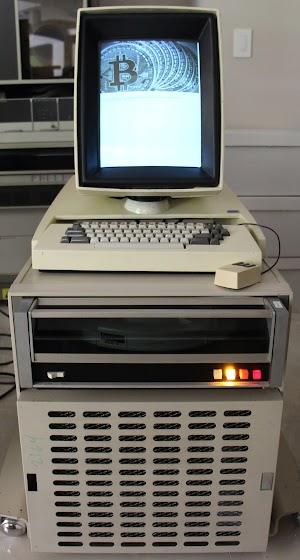
Bitcoin mining on a vintage Xerox Alto computer.

Bitcoin mining on a vintage Xerox Alto computer.

The Alto was a revolutionary computer designed at Xerox PARC in 1973 to investigate personal computing. It introduced high-resolution bitmapped displays, the GUI, Ethernet and laser printers to the world, among other things. In the photo above, the Alto computer is in the lower cabinet. The black box is the 2.5 megabyte disk drive. The Alto's unusual portrait display and an early optical mouse are on top.

How Bitcoin mining works

Bitcoin, a digital currency that can be transmitted across the Internet, has attracted a lot of attention lately. The Bitcoin system can be thought of as a ledger that keeps track of who owns which bitcoins, and allows them to be transferred from one person to another. The revolutionary feature of Bitcoin is there's no central machine or authority keeping track of things. Instead, the "blockchain" is stored across thousands of machines on the Internet, and the system works with nobody in charge.

To ensure everyone agrees on which transactions are valid, Bitcoin uses a process called mining—about every 10 minutes a block of outstanding transactions is mined, which makes the block "official". Bitcoin mining is designed to take an insanely huge amount of computational effort to mine a block, so nobody can take over the mining process. Miners compete against each other, generating trillions and trillions of "hashes" until someone finds a lucky one that succeeds in mining a block. It's hard to visualize just how difficult the hashing process is: finding a valid hash is less likely than finding a single grain of sand out of all the sand on Earth.

Bitcoin mining is based on cryptography, with a "hash function" that converts a block into an essentially random hash value. If the hash starts with 17 zeros,1 the block is successfully mined and is sent into the Bitcoin network. Most of the time the hash isn't successful, so the miner will modify the block slightly and try again, over and over billions of times. About every 10 minutes someone will successfully mine a block, and the process starts over. It's kind of like a lottery, where miners keep trying until someone "wins".

As a side-effect, mining adds new bitcoins to the system. For each block mined, miners currently get 12.5 new bitcoins (currently worth about $30,000) as well as fees, which encourages miners to do the hard work of mining blocks. With the possibility of receiving $30,000 every 10 minutes, miners invest in datacenters full of specialized mining hardware using huge amounts of electricity2.

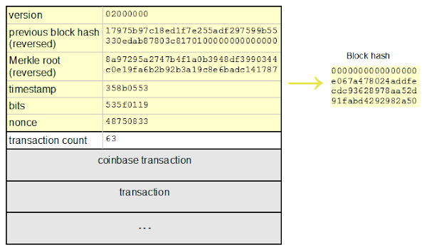
Structure of a Bitcoin block

Structure of a Bitcoin block. The data in yellow is hashed to yield the block hash, which becomes the identifier for the block. The block is linked to the previous block by including the previous block's hash, forming the blockchain. The Merkle root is a hash of all the transactions in the block.

The diagram above shows what actually goes into a block that is mined. The yellow part is the block header (which gets hashed), and it is followed by the transactions that go into the block. Each block contains the hash of the previous block, causing all the blocks to be linked together forming the blockchain. You can see that for the block above, the hash is successful because it starts with lots of zeros: 0000000000000000e067a478024addfecdc93628978aa52d91fabd4292982a50. The "Merkle root" is a hash of all the transactions that go into the block; this ensures that none of the mined transactions can be changed. The nonce is an arbitrary number; each attempt at mining the block changes the nonce.

To summarize the mining process: you collect new Bitcoin transactions and create a header (as in the diagram above). You do the cryptographic hash of the block. If by some incredible chance the result starts with 17 zeros you send the block into the Bitcoin network and "win" $30,000 in bitcoin. Otherwise, you change the nonce and try again. Probably none of the nonce values will work, so you change something else in the header and start over. If someone else succeeds in mining the block, you start over with the new previous block hash and new transactions.

I've simplified a lot of details above. For in-depth information on Bitcoin and mining, see my articles Bitcoins the hard way and Bitcoin mining the hard way.

The SHA-256 hash algorithm used by Bitcoin

Next, I'll discuss the hash function used in Bitcoin, which is based on a standard cryptographic hash function called SHA-256.3 The SHA-256 algorithm is so simple you can literally do it by hand, but it manages to scramble the data entirely unpredictably. The SHA-256 hash algorithm takes input blocks of 512 bits (i.e. 64 bytes), combines the data cryptographically, and generates a 256-bit (32 byte) output.

The SHA-256 algorithm consists of a simple round repeated 64 times. The diagram below shows one round, which takes eight 4-byte inputs, A through H, performs a few operations, and generates new values for A through H. As can be seen from the diagram above, only A and E are changed in a round, while the others are just shifted over. Even so, after 64 rounds the input data will be completely scrambled, generating the unpredictable hash output.

The SHA-256 algorithm is pretty simple, about a page of pseudocode and can be easily implemented on a computer, even one as old as the Alto, using simple arithmetic and logic operations.5

SHA-256 round, from Wikipedia

SHA-256 round, from Wikipedia created by kockmeyer, CC BY-SA 3.0.

The dark blue boxes mix up the values in non-linear ways that are hard to analyze cryptographically. (If you could figure out a mathematical shortcut to generate successful hashes, you could take over Bitcoin mining.) The Ch"choose" box chooses bits from F or G, based on the value of input E. The Σ"sum" boxes rotate the bits of A (or E) to form three rotated versions, and then sum them together. The Ma"majority" box looks at the bits in each position of A, B, and C, and selects 0 or 1, whichever value is in the majority. The red boxes perform 32-bit addition, generating new values for A and E. The input data enters the algorithm through the Wt values. The Kt values are constants defined for each round.4

Implementing SHA-256 in BCPL

I implemented SHA-256 in BCPL, a programming language that was a precursor to C. It's a lot like C with syntax changes, except the only type is 16-bit words. My SHA-256 code is in sha256.bcpl. The snippet below (the choose function) will give you an idea of what BCPL looks like. Each value is two words; BCPL does array access with !1 instead of [1]. Like C++, comments are indicated with a double slash. Unlike C, BCPL uses words for xor and not.

   // ch := (e and f) xor ((not e) and g)
   ch!0 = (e!0 & f!0) xor ((not e!0) & g!0)
   ch!1 = (e!1 & f!1) xor ((not e!1) & g!1)

The mining is done in bitcoin.bcpl: it creates a Bitcoin header (from hardcoded values), substitutes the nonce, and calls the SHA-256 code to hash the header twice. One interesting feature of the code is the structure definition for the Bitcoin header in BCPL (below), similar to a C struct. It defines a two word field for version, 16 words for prevHash, and so forth; compare with the Bitcoin structure diagram earlier. Interestingly, ^1,16 indicates an array with indices from 1 to 16 inclusive. BCPL is not 0-indexed or 1-indexed, but lets you start array indices at arbitrary values.7

structure HEADER:
[
version^1,2 word
prevHash^1,16 word
merkleRoot^1,16 word
timestamp^1,2 word
bits^1,2 word
nonce^1,2 word
]

The line shows how structures are accessed in BCPL; it initializes one word of the header, using the slightly strange BCPL syntax. >>HEADER sort of casts the header variable to the HEADER structure described earlier. Then .prevhash^1 accesses the first word of the prevhash field. Also note that #13627 is an octal value; BCPL inconveniently doesn't include hex constants.6

header>>HEADER.prevHash^1 = #13627

The screenshot below shows the output as the program runs. The number on the left is each nonce in sequence as it is tested. The long hex number on the right is the resulting hash value. Each nonce results in a totally different hash value, due to the cryptographic hash algorithm.

On the Alto screen, each line shows a nonce value and the resulting hash.

On the Alto screen, each line shows a nonce value and the resulting hash.

Performance

The Alto can hash about 1.5 blocks per second, which is exceedingly slow by Bitcoin standards. At this speed, mining a single block on the Alto would take about 5000 times the age of the universe The electricity would cost about 2x10^16 dollars. And you'd get 12.5 bitcoins (₿12.5) worth about $30,000. Obviously, mining Bitcoin on a Xerox Alto isn't a profitable venture.

In comparison, a USB stick miner performs 3.6 billion hashes per second. The Alto cost about $12,000 to manufacture in 1973 (about $60,000 in current dollars), while the stick miner costs $200. The Alto used hundreds of watts, while the stick minter uses about 4 watts. The enormous difference in performance is due to huge increase in computer speed since the 1970s described by Moore's law as well as the giant speed gain from custom Bitcoin mining hardware.

The Alto wasn't a particularly fast machine, performing about 400,000 instructions per second. The Alto's instruction set lacks many of the operations you'd find on a modern processor. For instance, the SHA-256 algorithm makes heavy use of Boolean operations including exclusive-OR and OR. These are pretty basic instructions that you'd find on even something as primitive as the 6502, but the Alto doesn't have them. Instead, these operations are implemented with an inefficient subroutine call that does a sequence of operations with the same effect.

In addition, SHA-256 heavily uses bit shift and rotate operations. Modern processors typically have a "barrel shifter" that lets you shift by as many bits as you want in one step. The Alto's shift instructions, on the other hand, only shift a single bit. Thus, to shift by, say 10 bits, the Alto code calls a subroutine that performs 10 separate shift instructions. The result is a shift operation is much slower than you might expect.

You can see the Alto's arithmetic-logic board below. The Alto didn't use a microprocessor but instead built a CPU from simple TTL chips. You can see that even providing single-bit shifts required 8 separate chips—it's not surprising that the Alto doesn't do more complex shift operations.

The Alto doesn't have a microprocessor, but a CPU built from individual TTL chips. The ALU board has chips for arithmetic, chips for shifting, and chips for registers.

The Alto doesn't have a microprocessor, but a CPU built from individual TTL chips. The ALU board has chips for arithmetic, chips for shifting, and chips for registers.

I should point out that I'm not trying to write the best possible mining code for the Alto, and there are plenty of optimizations that one could do.8 For instance, writing the code in microcode would speed it up considerably, but Alto microcode is very hard to understand, let along write. My blog post on generating the Mandelbrot set on the Alto discussed Alto performance optimizations in detail, so I won't say more about optimization here.

Conclusion

The screenshot below shows a successful hash, ending in a bunch of zeros9. (I also display an image to show off the Alto's high-resolution bitmapped display.) Since the Alto would take well beyond the lifetime of the universe to find a successful hash, you might wonder how I found this. For this demonstration I simply used as input a block that had been successfully mined in the past, specifically block #286819. Thus, the algorithm succeeded quickly, but since it was an old block, I didn't make any money off it.

The algorithm found a successful hash, indicated by all the zeros at the end. Bitcoin graphic source probably MoneyWeek.

The algorithm found a successful hash, indicated by all the zeros at the end. Bitcoin graphic source probably MoneyWeek.

My code is on github if you want to look at BCPL code or try it out.

Notes and references

  1. At current difficulty, about 1 in 3x10^21 hashes will be successful at mining a block; a valid hash must start with approximately 17 zeros. The mining difficulty changes periodically to keep the time between blocks at approximately 10 minutes. As mining hardware gets faster, the difficulty factor is automatically updated to make mining more difficult so miners can never really catch up. 

  2. A while back I estimated that Bitcoin mining uses about as much electricity as the entire country of Cambodia. One paper puts mining's energy consumption comparable to Ireland's electricity usage. 

  3. Bitcoin uses "double SHA-256" which simply consists of applying the SHA-256 function twice.  

  4. The K constants used in the SHA-256 algorithm are provided by the NSA. You might worry that the NSA cleverly designed these constants to provide a backdoor. However, to prove that these are just arbitrary random constants, the NSA simply used the cube roots of the first 64 primes. 

  5. While SHA-256 is easy to implement, that's not the case for all the cryptography used by Bitcoin. To create a Bitcoin transaction, the transaction must be signed with elliptic curve cryptography. This requires 256-bit modular arithmetic, which is about as hard as it sounds. Even a simple implementation is 1000 lines of C. I decided that porting this to BCPL was too much effort for me. 

  6. I wrote a simple Python script to convert the many 32-bit hexadecimal constants used by SHA-256 to 16-bit octal constants. It's a good thing that hex has almost entirely replaced octal, as it is much better. 

  7. Some people claim that BCPL arrays are 0-based. However, arrays in BCPL structures can start at an arbitrary value. I start with 1 because that's what the Alto code typically does. (This caused me no end of confusion until I realized the indices weren't zero-based.) 

  8. The code could be made 33% faster by taking advantage of an interaction between SHA-256 and the Bitcoin header structure. Bitcoin performs a SHA-256 hash twice on the 80-byte header. Since SHA-256 only handles 64 bytes at a time, the first hash requires two SHA-256 cycles. The second hash takes a third SHA-256 cycle. However, when mining, the only thing that changes from one attempt to the next is the nonce value in the header. It happens to be in the second half of the header, which means the SHA-256 cycle performed on the first half of the header can be done once and then reused. Thus, the double SHA-256 hash can be done with two SHA-256 cycles instead of three. Bitcoin mining usually performs this optimization, but I left it out of the code to make the code less confusing. 

  9. You might wonder why Bitcoin successful hashes start with a bunch of zeros, while the displayed hash ends with a bunch of zeros. The reason is that Bitcoin reverses the byte order of the SHA-256 output. If you look closely, you'll see that the displayed hash matches the hash in the Bitcoin block diagram if you reverse bytes (i.e. pairs of hex digits). 

Inside Intel's first product: the 3101 RAM chip held just 64 bits

$
0
0
Intel's first product was not a processor, but a memory chip: the 31011 RAM chip, released in April 1969. This chip held just 64 bits of data (equivalent to 8 letters or 16 digits) and had the steep price tag of $99.50.2 The chip's capacity was way too small to replace core memory, the dominant storage technology at the time, which stored bits in tiny magnetized ferrite cores. However, the 3101 performed at high speed due to its special Schottky transistors, making it useful in minicomputers where CPU registers required fast storage. The overthrow of core memory would require a different technology—MOS DRAM chips—and the 3101 remained in use in the 1980s.3

This article looks inside the 3101 chip and explains how it works. I received two 3101 chips from Evan Wasserman and used a microscope to take photos of the tiny silicon die inside.4 Around the outside of the die, sixteen black bond wires connect pads on the die to the chip's external pins. The die itself consists of silicon circuitry connected by a metal layer on top, which appears golden in the photo. The thick metal lines through the middle of the chip power the chip. The silicon circuitry has a grayish-purple color, but it largely covered by the metal layer. Most of the chip contains a repeated pattern: this is the 16x4 array of storage cells. In the upper left corner of the chip, the digits "3101" in metal identify the chip, but "Intel" is not to be found.

Die photo of the Intel 3101 64-bit RAM chip. Click for a larger image.

Die photo of the Intel 3101 64-bit RAM chip. Click for a larger image.

Overview of the chip

The 3101 chip is controlled through its 16 external pins. To select one of the chip's 16 words of memory, the address in binary is fed into the chip through the four address pins (A0 to A3). Memory is written by providing the 4-bit value on the data input pins (D1 to D4). Four data output pins (O1 to O4) are used to read memory; these pins are inverted as indicated by the overbar. The chip has two control inputs. The chip select pin (CS) enables or disables the chip. The write enable pin (WE) selects between reading or writing the memory. The chip is powered with 5 volts across the Vcc and ground pins.

The diagram below shows how the key components of the 3101 are arranged on the die. The RAM storage cells are arranged as 16 rows of 4 bits. Each row stores a word, with bits D1 and D2 on the left and D3 and D4 on the right. The address decode logic in the middle selects which row of storage is active, based on the address signals coming from the address drivers at the top. At the bottom, the read/write drivers provide the interface between the storage cells and the data in and out pins.

Block diagram of the 3101 RAM chip.

Block diagram of the 3101 RAM chip.

Transistors

Transistors are the key components in a chip. The 3101 uses NPN bipolar transistors, different from the MOS transistors used in modern memory chips. The diagram below shows one of the transistors in the 3101 as it appears on the die. The slightly different tints in the silicon indicate regions that have been doped to form N and P type silicon with different semiconductor properties. The cross-section diagram illustrates the internal structure of the transistor. On top (black) are the metal contacts for the collector (C), emitter (E), and base (B). Underneath, the silicon has been doped to form the N and P regions that make up the transistor.

A key innovation of the 3101 was using Schottky transistors (details), which made the 3101 almost twice as fast as other memory chips.5 In the cross section, note that the base's metal contact touches both the P and N regions. You might think this shorts the two regions together, but instead a Schottky diode is formed where the metal contacts the N layer.6

The structure of an NPN Schottky transistor inside the Intel 3101 chip.

The structure of an NPN Schottky transistor inside the Intel 3101 chip.

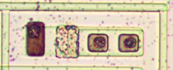
The 3101 also used many multiple-emitter transistors. While a multiple-emitter transistors may seem strange, they are common in bipolar integrated circuits, especially TTL logic chips. A multiple-emitter transistor simply has several emitter regions embedded in the base region. The die photo below shows one of these transistors with the collector on the left, followed by the base and two emitters.

A multiple-emitter transistor from the Intel 3101 chip.

A multiple-emitter transistor from the Intel 3101 chip.

Driving the data output pins requires larger, high-current transistors. The image below shows one of these transistors. The central rectangle is the base, surrounded by the C-shaped emitter in the middle and the large collector on the outside. Eight of these high-current transistors are also used to drive the internal address select lines.

For the high-current output, the Intel 3101 chip uses larger transistors.

For the high-current output, the Intel 3101 chip uses larger transistors.

Diodes

While examining the 3101 chip, I was surprised by the large number of diodes on the chip. Eventually I figured out that the chip used DTL (diode-transistor logic) for most of its logic rather than TTL (transistor-transistor logic) that I was expecting. The diagram below shows one of the diodes on the chip. I believe the chip builds diodes using the standard technique of connecting an NPN transistor as a diode.

Presumed structure of a diode inside the 3101 chip. I believe this is a regular diode, not a Schottky diode.

Presumed structure of a diode inside the 3101 chip. I believe this is a regular diode, not a Schottky diode.

Resistors

The die photo below shows several resistors on the 3101 die. The long, narrow snaking regions of p-type silicon provide resistance. Resistors in integrated circuits are inconveniently large, but are heavily used in the 3101 for pull-up and pull-down resistors. At the right is a square resistor, which has low resistance because it is very wide.7 It is used to route a signal under the metal layer, rather than functioning a resistor per se.

Resistors inside the 3101 chip.

Resistors inside the 3101 chip.

The static RAM cell

Now that I've explained the individual components of the chip, I'll explain how the circuitry is wired together for storage. The diagram below shows the cell for one bit of storage with the circuit diagram overlaid. Each cell consists of two multi-emitter transistors (outlined in red) and two resistors (at the top). The horizontal and vertical wiring connects cells together. This circuit forms a static RAM cell, basically a latch that can be in one of two states, storing one data bit.

The circuitry of one storage cell of the 3101 RAM chip. The two multiple-emitter transistors are outlined in red.

The circuitry of one storage cell of the 3101 RAM chip. The two multiple-emitter transistors are outlined in red.

Before explaining how this storage cell works, I'll explain a simpler latch circuit, below. This circuit has two transistors cross-connected so if one transistor is on, it forces the other off. In the diagram, the left transistor is on, which keeps the right transistor off, which keeps the left transistor on. Thus, the circuit will remain in this stable configuration. The opposite state—with the left transistor off and the right transistor on—is also stable. Thus, the latch has two stable configurations, allowing it to hold a 0 or a 1.

A simple latch circuit. The transistor on the left is on, forcing the transistor on the right off, forcing the transistor on the left off...

A simple latch circuit. The transistor on the left is on, forcing the transistor on the right off, forcing the transistor on the left off...

To make this circuit usable—so the bit can be read or modified—more complex transistors with two emitters are used. One emitter is used to select which cell to read or write, while the other emitter is used for the read or write data. This yields the schematic below, which matches the storage cell die photo diagram above.

The RAM cell used in the Intel 3101 is based on multiple-emitter transistors. The row select lines are raised to read/write the row of cells. Each data line accesses a column of cells.

The RAM cell used in the Intel 3101 is based on multiple-emitter transistors. The row select lines are raised to read/write the row of cells. Each data line accesses a column of cells.

Multiple storage cells are combined into a grid to form the memory memory. One word of memory consists of cells in the same row that share select lines. All the cells in a column store the same bit position; their data lines are tied together. (The bias line provides a voltage level to all cells in the memory.8)

Note that unlike the simplified cell, the circuit above doesn't have an explicit ground connection; to be powered, it requires a low input on either the select or data/bias lines. There are three cases of interest:

  • Unselected: If the negative row select line is low, current flows out through the row select line. The data and bias lines are unaffected by this cell.
  • Read: If the negative row select line is higher than the data and bias lines, current will flow out the data line if the left transistor is on, and out the bias line if the right transistor is on. Thus, the state of the cell can be read by examining the current on the data line.
  • Write: If the negative row select line is higher and the data and bias lines have significantly different voltages, the transistor on the lower side will switch on, forcing the cell into a particular state. This allows a 0 or 1 to be written to the cell.

Thus, by carefully manipulating the voltages on the select lines, data lines and the bias line, one row of memory can be read or written, while the other cells hold their current value without influencing the data line. The storage cell and the associated read/write circuitry are essentially analog circuits rather than digital since the select, data, and bias voltages must be carefully controlled voltages rather than logic levels.

The address decode logic

The address decode circuitry determines which row of memory cells is selected by the address lines.11 The interesting thing about this circuitry is that you can easily see how it works just by looking at the die photo. The address driver circuitry sends the four address signals along with their complements on eight metal traces through the chip. Each storage row has a four-emitter transistor. In each row you can see four black dots, which are the connections between emitters and address lines. A row will be selected if all the emitter inputs are high.9 A dot on an address line (e.g. A0) will "match" a 1, while a dot on the complemented address line (e.g. A0) will match a 0, so each row matches a unique four-bit address. In the die photo below, you can see the decoding logic counting down in binary for rows 15 down to 11;10 the remainder of the circuit follows the same pattern.

The address decode logic in the Intel 3101 RAM chip. Each row decodes matches four address lines to decode one of the 16 address combinations. You can see the value counting down in binary.

The address decode logic in the Intel 3101 RAM chip. Each row decodes matches four address lines to decode one of the 16 address combinations. You can see the value counting down in binary.

Some systems that used the 3101

The 64-bit storage capacity of the 3101 was too small for a system's main memory, but the chip had a role in many minicomputers. For example, the Burroughs D Machine was a military computer (and the source of the chips I examined). It used core memory for its main storage, but a board full of 3101 chips provided high-speed storage for its microcode. The Xerox Alto used four 3101 chips to provide 16 high-speed registers for the CPU, while the main memory used slower DRAM chips. Interdata used 3101 chips in many of its 16- and 32-bit minicomputers up until the 1980s.12

The 3101 was also used in smaller systems. The Diablo 8233 terminal used them as RAM.13 The Datapoint 2200 was a "programmable terminal" that held its processor stack in fast 3101 chips rather than the slow main memory which was built from Intel 1405 shift registers.

The CPU of the Datapoint 2200 computer was built from a board full of TTL chips. The four white chips in the lower center-right are Intel 3101 RAM chips holding the stack. Photo courtesy of Austin Roche (I think).

The CPU of the Datapoint 2200 computer was built from a board full of TTL chips. The four white chips in the lower center-right are Intel 3101 RAM chips holding the stack. Photo courtesy of Austin Roche (I think).

How I created the die photos

To get the die photos, I started with two chips that I received thanks to Evan Wasserman and John Culver. The pins on the chips had been crushed in the mail, but this didn't affect the die photos. The chips had two different lot numbers that indicate they were manufactured a few months apart. Strangely, the metal lids on the chips were different sizes and the dies were slightly different. For more information, see the CPU Shack writeup of the 3101.

Two 3101 RAM chips. The chip on the right was manufactured slightly later and has a larger lid over the die.

Two 3101 RAM chips. The chip on the right was manufactured slightly later and has a larger lid over the die.

Popping the metal lid off the chips was easy—just a tap with a hammer and chisel. This revealed the die inside.

With the lid removed, you can see the die of the 3101 RAM chip and the bond wires connected to the die.

With the lid removed, you can see the die of the 3101 RAM chip and the bond wires connected to the die.

Using a metallurgical microscope and Hugin stitching software (details), I stitched together multiple microscope photos to create an image of the die. The metal layer is clearly visible, but it obscures the silicon underneath, making it hard to determine the chip's circuitry. The photo below shows a closeup of the die showing the "3101" part number.

The die photo of the Intel 3101 shows mostly the metal layer.

The die photo of the Intel 3101 shows mostly the metal layer.

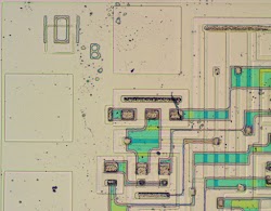
I applied acid14 to remove the metal layer. This removed most of the metal, revealing the silicon circuitry underneath. Some of the metal is still visible, but thinner, appearing transparent green. Strangely, the number 3101 turned into 101; apparently the first digit wasn't as protected by oxide as the other digits.

Treatment with acid dissolved most of the metal layer of the 3101 chip, revealing the silicon circuits underneath.

Treatment with acid dissolved most of the metal layer of the 3101 chip, revealing the silicon circuits underneath.

Below is the complete die photo of the chip with the metal layer partially stripped off. (Click it for a larger version.) This die photo was most useful for analyzing the chip. Enough of the metal was removed to clearly show the silicon circuits, but the remaining traces of metal showed most of the wiring. The N+ silicon regions appear to have darkened in this etch cycle.

Die photo of the Intel 3101 64-bit RAM chip with metal layer partially stripped off.

Die photo of the Intel 3101 64-bit RAM chip with metal layer partially stripped off.

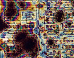
I wanted to see how the chip looked with the metal entirely removed so I did a second etch cycle. Unfortunately, this left the die looking like it had been destroyed.

After dissolving most of the oxide layer, the die looks like a mess. (This is a different region from the other photos.)

After dissolving most of the oxide layer, the die looks like a mess. (This is a different region from the other photos.)

I performed a third etch cycle. It turns out that the previous etch hadn't destroyed the die, but just left a thin layer of oxide that caused colored interference bands. The final etch removed the remaining oxide, leaving a nice, clean die. Only a ghost of the "101" number is visible. The contacts between the metal layer and the silicon remained after the etch; they may be different type of metal that didn't dissolve.

The metal and oxide have been completely removed from the 3101 die, showing the silicon layer.

The metal and oxide have been completely removed from the 3101 die, showing the silicon layer.

Below is the full die photo with all the metal stripped off. (Click it for a full-size image.)

Die photo of the Intel 3101 64-bit RAM chip with metal layer stripped off.

Die photo of the Intel 3101 64-bit RAM chip with metal layer stripped off.

Conclusion

The 3101 RAM chip illustrates the amazing improvements in integrated circuits driven by Moore's Law.15 While the 3101 originally cost $99.50 for 64 bits, you can now buy 16 gigabytes of RAM for that price, two billion times as much storage. If you built a 16 GB memory from two billion 3101 chips, the chips alone would weigh about 3000 tons and use over a billion watts, half of Hoover Dam's power. A modern 16GB DRAM module, in comparison, uses only about 5 watts.

As for Intel, the 3101 RAM was soon followed by many other memory products with rapidly increasing capacity, making Intel primarily a memory company that also produced processors. However, facing strong competition from Japanese memory manufacturers, Intel changed its focus to microprocessors and abandoned the DRAM business in 1985.16 By 1992, the success of the x86 processor line had made Intel the largest chip maker, justifying this decision. Even though Intel is now viewed as a processor company, it was the humble 3101 memory chip that gave Intel its start.

Thanks to Evan Wasserman and John Culver for sending me the chips. John also did a writeup of the 3101 chip, which you can read at CPU Shack.

Notes and references

  1. You might wonder why Intel's first chip had the seemingly-arbitrary number 3101. Intel had a highly-structured naming system. A 3xxx part number indicated a bipolar product. A 1 for the second digit indicated RAM, while the last two digits (01) were a sequence number. Fortunately, the marketing department stepped in and gave the 4004 and 8008 processors better names. 

  2. Memory chips started out very expensive, but prices rapidly dropped. Computer Design Volume 9 page 28, 1970, announced a price drop of the 3101 from $99.50 to $40 in small volumes. Ironically, the Intel 3101 is now a collector's item and on eBay costs much more than the original price—hundreds of dollars for the right package. 

  3. Severalsources say that the 3101 was the first solid state memory, but this isn't accurate. There were many companies making memory chips in the 1960s. For instance, Texas Instruments announced the 16-bit SN5481 bipolar memory chip in 1966 (Electronics, V39 #1, p151) and Transitron had the TMC 3162 and 3164 16-bit RAM (Electrical Design News, Volume 11, p14). In 1968, RCA made 72-bit and 288-bit CMOS memories for the Air Force (document, photo). Lee Boysel built 256-bit dynamic RAMs at Fairchild in 1968 and 1K dynamic RAMs at Four Phase Systems in 1969 (timeline and Boysel presentation). For more information on the history of memory technology, see timeline and History of Semiconductor Engineering, p215. Another source for memory history is To the Digital Age, p193. 

  4. From my measurements, the 3101 die is about 2.39mm by 3.65mm. Feature size is about 12µm. 

  5. If you've used TTL chips, you probably used the 74LSxx family. The "S" stands for the Schottky transistors that make these chip fast. These chips were "the single most profitable product line in the history of Texas Instruments" (ref). 

  6. The Schottky diode in the Schottky transistor is formed between the base and collector. This diode prevents the transistor from becoming saturated, allowing it to switch faster. 

  7. The resistance of an IC resistor is proportional to the length divided by the width. The sheet resistance of a material is measured in the unusual unit of ohms per square. You might think it should be per square nanometer or square mm or something, but since the resistance depends on the ratio of length to width, the unit cancels out. 

  8. The bias line is shared by all the cells. For reading, it is set to a low voltage. For writing, it is set to an intermediate voltage: higher than the data 0 voltage, but lower than the data 1 voltage. The bias voltage is controlled by the write enable pin.

    More advanced chips use two data lines instead of a bias line for more sensitivity. A differential amplifier to compare the currents on the two data lines and distinguish the tiny change between a zero bit and a one bit. However, the 3101 uses such high currents internally that this isn't necessary; it can read the data line directly. 

  9. If my analysis is correct, when a row is selected, the address decode logic raises both the positive row select and negative row select lines by about 0.8 volts (one diode drop). Thus, the cell is still powered by the same voltage differential, but the voltage shift makes the data and bias lines active. 

  10. Address lines A3 and A2 are reversed in the decoding logic, presumably because it made chip layout simpler. This has no effect on the operation of the chip since it doesn't matter of the physical word order matches the binary order. 

  11. The 3101 has a chip select pin that makes it easy to combine multiple chips into a larger memory. If this pin is high, the chip will not read or write its contents. One strange thing about the address decoding logic is that each pair of address lines is driven by a NAND gate latch. There's no actual latching happening, so I don't understand why this circuit is used.

    How the 3101 implements this feature is a bit surprising. The chip select signal is fed into the address decoding circuit; if the chip is not selected, both A0 and the complement A0 are forced low. Thus, none of the rows will match in the address decoding logic and the chip doesn't respond. 

  12. The Interdata 7/32 (the first 32-bit minicomputer) used 3101 chips in its memory controller. (See the maintenance manual page 338.) The Interdata 16/HSALU used 3101 chips for its CPU registers. (See the maintenance manual page 259.) As late as 1982, the Interdata 3210 used 3101 chips to hold cache tags (see manual page 456). On the schematics note that part number 19-075 indicates the 3101. 

  13. The Diablo 8233 terminal used 3101A (74S289) chips as RAM for its discrete TTL-based processor (which was more of a microcontroller) that controlled the printer. (See maintenance manual page 187.) This systems was unusual since it contained both an 8080 microprocessor and a TTL-based processor. 

  14. The metal layer of the chip is protected by silicon dioxide passivation layer. The professional way to remove this layer is with dangerous hydrofluoric acid. Instead, I used Armour Etch glass etching cream, which is slightly safer and can be obtained at craft stores. I applied the etching cream to the die and wiped it for four minutes with a Q-tip. (Since the cream is designed for frosting glass, it only etches in spots. It must be moved around to obtain a uniform etch.) Next, I applied a few drops of hydrochloric acid (pool acid from the hardware store) to the die for a few hours. 

  15. Moore's law not only describes the exponential growth in transistors per chip, but drives this growth. The semiconductor industry sets its roadmap according to Moore's law, making it in some sense a self-fulfilling prophecy. See chapter 8 of Technological Innovation in the Semiconductor Industry for a thorough discussion. 

  16. Intel's 1985 Annual Report says "It was a miserable year for Intel" and discusses the decision to leave the DRAM business. 

Examining a vintage RAM chip, I find a counterfeit with an entirely different die inside

$
0
0
A die photo of a vintage 64-bit TTL RAM chip came up on Twitter recently, but the more I examined the photo the more puzzled I became. The chip didn't look at all like a RAM chip or even a TTL chip, and in fact appeared partially analog. By studying the chip's circuitry closely, I discovered that this RAM chip was counterfeit and had an entirely different die inside. In this article, I explain how I analyzed the die photos and figured out what it really was.

The die photo above is part of Project 54/74, an ambitious project to take die photos of every chip in the popular 7400 series of TTL chips (and the military-grade 5400 versions). The 74LS189 was an early RAM chip (1976) that held just 64 bits: sixteen 4-bit words. This photo interested me because I had recently written about Intel's first product, the 64-bit 3101 memory chip (1969). In my photo below of the 3101, you can see the 16 rows and 4 columns of memory cells forming a regular pattern that takes up most of the chip. The 74LS189 was an improved version of the 3101 RAM chip, so the two die photos should have been very similar. But the two photos were entirely different and the 74LS189 die didn't have 64 of anything. This just didn't make sense.

Die photo of the Intel 3101 64-bit RAM chip. Click for a larger image.

Die photo of the Intel 3101 64-bit RAM chip. Click for a larger image.

A closer examination of the chip brought more confusion. I usually start analyzing a chip by figuring out which of the pins are power, inputs, and outputs, and cross-referencing with the datasheet to find the function of each pin. The power and ground pins are easy to spot, since these are connected to thick metal traces that feed every part of the chip. Most 7400-series chips have the power and ground on diagonally-opposite corners of the chip.1 The die photo, however, shows the power and ground separated by just 5 positions. This immediately rules out the possibility that the chip is the advertised 74LS189, and makes it unlikely to be a 7400-series chip at all. In addition, the transistors all looked wrong. A chip in the 74LSxx series is built from bipolar transistors, which are fairly large and have a distinctive appearance. The transistors in the die photo looked like much smaller and simpler CMOS transistors.

Some visible features on the die of the alleged 74LS189 chip. These features don't match a RAM chip.

Some visible features on the die of the alleged 74LS189 chip. These features don't match a RAM chip.

The chip also contained a complex resistor network, not the simple resistors you'd expect on a TTL chip. The resistor network (along with the large, complex transistors next to it) led me to suspect that this chip had analog circuitry as well as digital logic. I thought it might be an analog-to-digital converter (ADC), but after looking at some ADC datasheets, I decided that wasn't the case. The chip had way too many inputs, for one thing.

The first big clue was when I studied the resistor network carefully. In the photo below, I've marked the resistors with light or dark blue lines. They are all exactly the same length, giving them the same resistance (R). Some were connected as pairs to get a resistance of exactly 2R. I noticed they were connected in a pattern of R-2R-R-2R-... which forms a R-2R resistor ladder network. This structure is used for digital to analog conversion (DAC): you feed bits into the network and you get out a voltage corresponding to the value. The chip had two of these ladders, forming two 4-bit digital-to-analog converters.

The resistors in the center of the die forms two R-2R ladders, which are simple digital-to-analog converters.

The resistors in the center of the die forms two R-2R ladders, which are simple digital-to-analog converters.

What values were going into the digital-to-analog converters? The middle of the die photo contained two small matrices, which I recognized as ROMs, each holding about 24 four-bit words. Perhaps the values in the ROMs were being fed to the DAC. Each row of the ROM had one section (on the right below) to decode 5 address bits, and a second section (on the left) to output the associated 4 data bits. Each data row has a transistor for 1 or no transistor for 0. The decoder is arranged in pairs with one transistor present out of each pair, either matching a 0 address or matching a 1 address. Thus, by looking at the chip, we can read the values in the ROMs.

Detail of a ROM in the chip. Each row stores four bits of data. The pattern of square metal contacts shows the data bits. On the right, the address decode circuit matches the address for the row.

Detail of a ROM in the chip. Each row stores four bits of data. The pattern of square metal contacts shows the data bits. On the right, the address decode circuit matches the address for the row.

Normally a ROM has sequential rows, so you can see the decoder counting in binary, but this decoder was different. Addresses in the ROM were arranged as 10011, 11001, 01100, ... Each address was generated by shifting the previous one to the right and adding a new bit on the left. E.g. 10011 -> 11001. This suggested the ROM addresses were generated by a linear-feedback shift register (LFSR) rather than a binary counter. The motivation is a shift register takes up less space than a counter on the chip; if you don't need the counter to count in the normal order, this is a good tradeoff. There were a couple strange things about the ROM: some addresses appeared to be missing and some addresses perform sort of a "wild card" match, but I'll ignore that for now. Also, the two ROMs were similar but not quite identical.

Looking at the data in the ROM, I noticed the rightmost bit was present for a while, then absent, and finally present again, while the other bits jumped around. That suggested the rightmost bit was the high-order bit. I extracted the data, and after swapping a couple bits got the curve below, a somewhat distorted sine wave.

By visually reading the values from the ROM, we can extract a waveform. But it's strangely distorted

By visually reading the values from the ROM, we can extract a waveform. But it's strangely distorted

So, the mystery chip had two ROMs with sine-ish curves and two digital-to-analog converters. Clearly it's not a RAM chip, but what is it? I looked at function/waveform generator chips, but they didn't seem to match. Could it be a sound synthesis chip (like the 76477 or a Yamaha sythesizer chip)? They didn't seem to match the chip's characteristics either. Why would the chip have a bunch of inputs and an output with two sine wave channels? After puzzling for a long time, I thought of Touch-Tone phone dialing.

DTMF: dialing a Touch-Tone phone

Perhaps I should explain how Touch-Tone phones work. Technically known as Dual-Tone Multi-Frequency signaling (DTMF), Touch-Tone was introduced in 1963 to replace rotary-dial phones with push button dialing. Each button press generates two tones of specific frequencies, which indicate the pressed button to the telephone switching system. Specifically, there is one tone for each row on the keypad and one tone for each column, and a button generates the two corresponding tones.2

A Touch-Tone telephone. Photo courtesy of Retero00064.

A Touch-Tone telephone. Photo courtesy of Retero00064.

Mostek introduced the MK5085 Touch-Tone dialer chip in 1975.3 This chip revolutionized the construction of Touch-Tone phones: instead of using eight carefully-tuned, expensive oscillators, the phone could generate the tones with a cheap integrated circuit. The MK5085 was soon followed by a series of Mostek integrated dialer chips with slightly different functions4 as well as versions from other manufacturers.5

A quick web search found a Touch-Tone chip datasheet. The pinout of this chip matched the die photo with the power, input and output pins in the right places. The datasheet said the chip was metal-gate CMOS (not TTL), which matched the appearance of the die. Finally, the datasheet's block diagram matched the functional blocks I could see on the chip.

Package of the counterfeit memory chip, labeled 74LS189. Courtesy of Robert Barauch.

Package of the counterfeit memory chip, labeled 74LS189. Courtesy of Robert Barauch.

This was pretty conclusive: the mystery die was not a RAM chip but an entirely unrelated DTMF dialing chip. This 74LS189 chip was counterfeit; someone had relabeled the DTMF die as a Texas Instruments 74LS189 chip.

How the DTMF chip works

Now that I had identified the chip, I wanted to understand more about how it works. It turns out that it uses some interesting mathematics and circuitry to generate the tones. The chip needs to generate two tones of the right frequencies based on the 4 row inputs and 4 column inputs from the keypad. It generates these tones by starting with a 3.579545 MHz11 frequency and dividing it down to two lower frequency clocks. Each clock is used to step through the sine-wave lookup table in ROM, generating a sine wave of the desired frequency. Finally, the two sine waves are mixed together to produce the output.

By looking at the output frequencies listed in the datasheet, we can deduce what is happening internally. For instance, to generate the 1639.0 Hz tone, you can divide the 3.579545 MHz input by 2184. (Reducing a frequency by an integer factor is straightforward in hardware: count the input pulses and reset every time you reach 2184.) Similarly, the other output frequencies can be generated by dividing by integers 2408, 2688, 2968, 3808 4200, 4648 and 5152. Dividing by numbers this large would require inconveniently large counters, but but I noticed these numbers are are all divisible by 56, yielding quotients 39, 43, 48, 53, 68, 75, 83 and 92. These smaller numbers are much more practical to divide by in hardware.

This suggests a straightforward hardware implementation: divide the 3.579545 MHz clock by 2. Then divide by 68, 75, 83 or 92 (depending on the row input), using a 7-bit counter. Finally, iterate through a 28-word ROM to generate the sine wave, yielding the 28-step sine wave described in the datasheet. Similarly, the column frequencies can be generated by dividing by 39, 43, 48 or 53 (using a 6-bit counter) depending on the column input.

At this point, I had reverse-engineered how the chip operated. Or had I? A closer look at the chip revealed 5-bit and 6-bit counters, one bit too small for the necessary divisors. What was going on? How could the chip divide by 68 with a 6-bit counter?

The diagram below shows divider circuitry for the row output, showing the 6-bit shift-register counter. Also visible is the circuit to detect when the counter should be reset, based on which of the four keypad rows is selected.7 The column circuitry is similar, but with a 5-bit counter.

Divider circuitry for the row signal, on the lower right of the die. The input frequency is divided by a particular value depending on which of the four keyboard rows is selected. The counter is implemented with a shift register. The LFSR logic generates the new bit shifted in. The count end check circuitry controls the count length for the selected row. The single button check verifies that exactly one button is pressed.

Divider circuitry for the row signal, on the lower right of the die. The input frequency is divided by a particular value depending on which of the four keyboard rows is selected. The counter is implemented with a shift register. The LFSR logic generates the new bit shifted in. The count end check circuitry controls the count length for the selected row. The single button check verifies that exactly one button is pressed.

More investigation showed that multiple companies made pin-compatible DTMF chips, but they all generated slightly different frequencies. 5 Although the chips seemed like clones, they were all implemented in different ways, dividing the input frequency differently, yielding outputs that were unique (but all within the phone system's tolerance). By repeating the mathematical analysis, I could reverse-engineer each manufacturer's implementation and figure out the divisors and ROM sizes. (Details in footnotes.10)

I found that the divisors for the MK5089 design would fit in the counters I saw on the chip. Specifically, it divides the input frequency by 4 and then divides row frequencies by 33, 36, 40 or 44 (values that fit in 6 bits) and the column frequencies by 17, 19, 21 or 23 (values that fit in 5 bits). The row output ROM has 29 values, while the column output ROM has 32 values. This nicely fit the counter sizes I saw on the die. It also explains why the two ROMs on the die are slightly different.8

Understanding the silicon

I reverse-engineered parts of the chip by closely examining the silicon circuits, so I'll explain some of the silicon-level structures. The chip is built mostly from CMOS13, but the structures are a bit more complex than you see in textbooks. The basic idea of CMOS is it is built from MOS transistors, both PMOS and NMOS transistors connected in a Complementary way (thus the name CMOS). To oversimplify, an NMOS transistor turns on when the input is high, and can pull the output low. A PMOS transistor is opposite; it turns on when the input is low, and can pull the output high.

The diagram below shows the structure of a metal-gate MOS transistor. Electricity flows between the source and the drain, under control of the gate. The metal gate is separated from the silicon by an insulating oxide layer. (The Metal / Oxide / Silicon layers give it the name MOS.) For a PMOS transistor, the source and drain are P-type silicon while the base silicon is N-type. An NMOS transistor is opposite: the source and drain are N-type silicon while the base silicon is P-type.

A metal-gate MOSFET transistor.

A metal-gate MOSFET transistor.

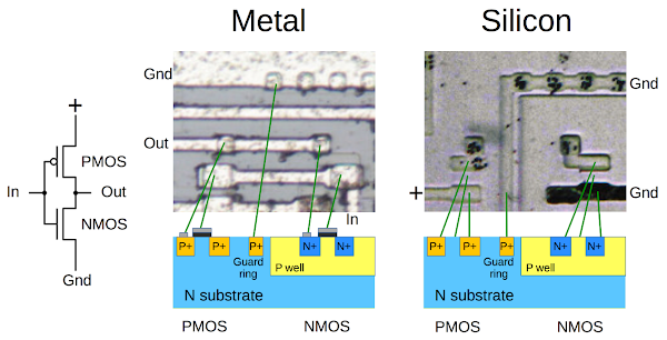
The diagram below shows a CMOS inverter on the chip, built from a PMOS transistor and an NMOS transistor. The first photo shows the metal layer. By dissolving the metal in acid, the silicon is revealed in the second photo. In combination, they reveal the inverter's structure, as shown in the cross-section diagram. You can see the metal gates for the PMOS and NMOS transistors, as well as the silicon regions for the source and drain.12 The black spots are contacts between the metal and silicon, where they are connected.

A CMOS inverter is built from a PMOS transistor and an NMOS transistor.

A CMOS inverter is built from a PMOS transistor and an NMOS transistor.

Note that the NMOS transistor must be embedded in P-type silicon. To achieve this, the transistor is placed in a "P well", a region of P-doped silicon. A grounded "guard ring" surrounds the P well to help isolate it. The chip contains multiple P wells, which typically hold multiple NMOS transistors.

Logic gates (NAND, NOR) are constructed by combining multiple transistors in a similar way (details). CMOS transistors can also be configured to pass or block a signal (details), a technique used to build the shift registers in the chip. These circuits are straightforward to recognize if you examine the chip closely, allowing the circuitry to be reverse engineered, for example the shift-register counter shown earlier.

The DMTF chip is both digital and analog. The diagram below shows the 4-bit digital-to-analog converter for the column tone. (This circuit is in the upper-left of the die; the similar row tone circuit is in the upper right.) The circuit takes 4 bits from the ROM, passes them through a buffer, and then four transistors drive the R-2R resistor ladder digital-to-analog converter that was discussed earlier. The resulting analog voltage forms the synthesized sine wave. Note that the transistors are scaled to provide the necessary current; the "8x" transistor is eight times the size of the "1x" transistor. The NMOS transistors are in a P-well, as described earlier.

This circuit on the DMTF chip converts a 4-bit digital value from the ROM into an analog voltage.

This circuit on the DMTF chip converts a 4-bit digital value from the ROM into an analog voltage.

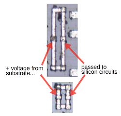
The die has some unusual structures, metal squares and larger loops that at first glance don't seem connected to anything. I've never seen these described before, so I'll explain what they are. They provide power and ground to parts of the circuit without direct wiring to the power or ground pins. Integrated circuits typically have extensive wiring in the metal layer to provide power and ground to all the circuits that need them. This chip, however, eliminates some of this wiring by using the substrate as a power connection and using the guard rings as ground connections. The photo below shows metal loops that provides a bridge between the positive substrate and a circuit that requires positive voltage.

Metal loops are used to get positive voltage (Vcc) from the substrate and feed it to circuits that need it.

Metal loops are used to get positive voltage (Vcc) from the substrate and feed it to circuits that need it.

The metal loops below provide a bridge between the negative guard ring and the circuitry that requires ground. As far as I can tell, there's no reason to make these links a loop rather than a straight connection.

Metal loops connect the guard ring (at ground potential) to circuits that need a ground connection.

Metal loops connect the guard ring (at ground potential) to circuits that need a ground connection.

Conclusion

The chip turned out to be a Touch-Tone DTMF dialer, most likely a knockoff MK5089, repackaged as a 74LS189 RAM chip. Why would someone go to the effort of creating counterfeit memory chips that couldn't possibly work? The 74LS189 is a fairly obscure part, so I wouldn't have expected counterfeiting it to be worth the effort. The chips sell for about a dollar on eBay, so there's not a huge profit opportunity. However, IC counterfeiting is a widespread problem14. For instance, 15% of replacement semiconductors purchased by the Pentagon are estimated to be counterfeit. With counterfeiting this widespread, even an obscure chip like the 74LS189 can be a target.

As for Robert Baruch's purchase of the chip, he contacted the eBay seller who gave him a refund. The seller explained that the chip must have been damaged in shipping! (Clearly you should pack your chips carefully so they don't turn into something else entirely.)

Thanks to Robert Baruch for the die photos. His high-resolution photos are here and here.

Notes and references

  1. A few unusual 7400-series chips (such as the 7473 flip flop) don't have the power and ground pins diagonally opposite, but in the middle. On the die, however, these pins are still symmetrically opposite. This simplifies routing of power and ground on the die. 

  2. Touch-Tone keypads normally have four rows and three columns, but the system supports a fourth column. The fourth column is used for some special network purposes and require a special keypad. 

  3. The Touch-Tone chip waspatented, which later led to a complex patent battle

  4. Mostek later introduced a second generation of dialer chips with the MK5380. Instead of an R-2R A/D converter, it used a network of resistors with taps selected to generate the sinusoidal voltages. That is, instead of using a ROM to fit the sine curve to 16 uniform voltage steps, 16 unequal voltage levels were selected to fit the sine curve. This was described in patent 4,446,436. The datasheet for the NTE1690 chip says it uses a "resistive ladder network", which is probably the same thing. 

  5. Many manufacturers made Touch-Tone chips that were compatible with the MK5089, often giving them similar part numbers. Some of them are TP5089, MV5089, UM95089, TCM5089, MK5089, and NTE1690 chips. While these DTMF chips seem interchangeable, surprisingly they use entirely different designs internally. Careful examination of the datasheets shows that they output slightly different frequencies. For instance, for the lowest tone the TP5089 has a frequency of 694.8 Hz, while the S2559 outputs 699.1 Hz and the NTE1690 outputs 701.3 Hz, all slightly off from the official 697 Hz.  

  6. Touch-Tone keypads have an unusual internal structure. A standard calculator keypad has a grid of switches. In contrast, a Touch-Tone keypad has 8 switches (4 row, 4 column) and each button closes two switches (so it is known as 2-of-8). Thus, while a calculator normally scans the rows and reads the columns, the output of a Touch-Tone keypad can be read directly. Some DTMF chips include scanning circuitry so a calculator-style keypad can be used. 

  7. Conceptually, the counter is reset when the appropriate value is reached. However, since it is implemented with a linear-feedback shift register, only the input bit can be changed, rather than resetting entirely. That is, the counter jumps ahead (by one bit flip) at the proper point so the number of counts is the desired value. Strictly speaking, this makes the counter a nonlinear-feedback shift register. 

  8. My original readout of the ROM gave a distorted sine wave, but with further analysis I figured out the problem. I had noticed that the address patterns didn't always follow the shifted sequence from the LFSR. In addition, some addresses weren't fully decoded, in effect providing "wild card" addresses. Looking more closely, I realized that the wild card addresses would fill in the gaps in the sequence. The reason was that the ROM designers had used a shortcut to make the ROM smaller. For example, if address 00111 stored the value 13 and address 00011 also stored the value 13, these two rows in the ROM could be collapsed into one: decoding the address 00?11 to the value 13. (Strictly speaking, this makes it a PLA, not a ROM.) Essentially, the ROM could sometimes combine the same value on the ascending and descending parts of the sine way. When I filled in the missing entries, the resulting sine waves looked much better. This also showed that the two ROMs held 29 and 329 entries (as required by the mathematics) and explained why the two ROMs were slightly different on the die. 

  9. You might know that a LFSR will get stuck on all-zeros, so it can only use 2^n-1 of the possible 2^n values. So how can the chip's 5-bit LFSR access all 32 entries in the ROM? The solution is that it's a non-linear feedback shift register (NLFSR), slightly more complicated than a LFSR. In particular, there is a row in the PLA that detects the all-zero entry and keeps the sequence from getting stuck there (as would happen on a LFSR). 

  10. Each DTMF chip's datasheet lists slightly different output frequencies. By factoring these frequencies, I could reverse-engineer the internal design of the chip—the divisors it used and the ROM sizes. The table below gives these values for four different chip designs. Each output frequency is generated by dividing the crystal frequency (3.579545 MHz) by the scale factor, the appropriate divisor, and the points per cycle. Note that the output frequencies are all close to the correct frequencies, but not an exact match.

    ChipRow divisors and frequenciesColumn divisors and frequenciesPoints per cycleScale factor
    TP50899283756853484339282
    694.8 Hz770.1 Hz852.3 Hz940.0 Hz1206.0 Hz1331.7 Hz1486.5 Hz1639.0 Hz
    S25598073665946423834322
    699.1 Hz766.2 Hz847.4 Hz948.0 Hz1215.9 Hz1331.7 Hz1471.9 Hz1645.0 Hz
    MK5089, MV5089444036332321191729 (row), 32 (col)4
    701.3 Hz771.5 Hz857.2 Hz935.1 Hz1215.9 Hz1331.7 Hz1471.9 Hz1645.0 Hz
    UM950898073665946423834164
    699.1 Hz766.2 Hz847.4 Hz948.0 Hz1215.9 Hz1331.7 Hz1471.9 Hz1645.0 Hz
    Correct frequency:697 Hz770 Hz852 Hz941 Hz1209 Hz1336 Hz1477 Hz1633 Hz
     
  11. You might wonder why they picked 3.579545 MHz for the crystal, as that seems like a strange frequency. That's the NTSC colorburst frequency, used by color televisions for complex technical reasons. Since the crystals were made by the millions for color televisions, they were inexpensive and easy to obtain. 

  12. In the die photo, the source of an NMOS transistor connected to ground is much darker. I assume this is due to a different doping level, perhaps to pull the P well to ground. 

  13. While most of the circuitry in the chip is CMOS, other parts use NMOS or PMOS logic to simplify the circuitry. For instance, the ROMs have NMOS transistors for the address decode and PMOS for the data storage. Another example is the circuitry to detect multiple button presses. For the four row buttons, there are six double-press combinations which are detected by an AND-OR-INVERT gate with 6 AND gates. This is built as a single complex NMOS gate, with a pull-up resistor. The diagram below shows how it is structured. (A similar circuit checks the column inputs for double presses.)

    The circuitry to detect multiple button presses is built from NMOS, not CMOS.

    The circuitry to detect multiple button presses is built from NMOS, not CMOS.
  14. Two interesting articles about finding counterfeit semiconductors come from SparkFun and Bunnie Studios. For articles on counterfeiting, see this and this

Inside the vintage Xerox Alto's display, a tiny lightbulb keeps it working

$
0
0
In this Alto restoration episode, we repaired a second CRT display, exercising our TV repair skills and discovering a tiny mysterious lightbulb that caused the display to fail in a strange way. For those just tuning in, the Alto was a revolutionary computer designed at Xerox PARC in 1973 to investigate personal computing. It introduced the GUI, high-resolution bitmapped displays, WYSIWYG editors, Ethernet and laser printers to the world, among other things.

The YCombinator Xerox Alto, running a Mandelbrot set program I wrote in BCPL.

The YCombinator Xerox Alto, running a Mandelbrot set program I wrote in BCPL.

I've been restoring an Alto from YCombinator, along with Marc Verdiell, Carl Claunch and Luca Severini. Since we have the YCombinator Alto working (above), we've been trying trying to get a second Xerox Alto system running; this one is from DigiBarn. My full set of Alto posts is here and Marc's videos are here.

Inside the Alto's display

When we tried to connect the DigiBarn display to the Alto, we ran into a problem—it had an incompatible connector. Looking inside the display (below), we were surprised to find this connector led to a circuit board with a 6502 microprocessor; since the Alto came out in 1973 and the 6502 in 1975, this didn't make sense. After some investigation, I determined that although the display looked like an Alto display, it was actually for a Dorado, a Xerox minicomputer from 1979 that followed the Alto.

Inside the Xerox Alto's display. With the cover removed, the CRT and monitor circuitry are visible. The 7-wire interface board is at bottom-left. The Alto itself is in the cabinet under the display.

Inside the Xerox Alto's display. With the cover removed, the CRT and monitor circuitry are visible. The 7-wire interface board is at bottom-left. The Alto itself is in the cabinet under the display.

The Dorado was much faster than the Alto because the Dorado used ECL chips, the same technology used in the Cray-1 supercomputer. Unfortunately, since ECL chips used a lot of power and needed powerful cooling fans, the Dorado was too hot and noisy to use in an office. Putting a soundproof enclosure around the Dorado didn't work, so Xerox ended up putting Dorados in machine rooms. The user's keyboard, mouse and display was connected to the remote Dorado with a special cable using the "7-wire protocol" that Xerox invented for this purpose. The 6502 board was the interface for this protocol. 5

To connect the Alto to this display, I built an adapter cable that bypassed the 7-wire board. We hooked up the monitor, powered it on, and were greeted with a empty black screen. Given the age of the monitor, we weren't surprised that it didn't work. However, when we powered off the monitor, we saw a perfect image for a fraction of a second before the image collapsed to a dot and disappeared. This was unexpected—the monitor didn't work at all when powered on, but worked fine (but very briefly) when turned off! What could be going on?

How a CRT monitor works

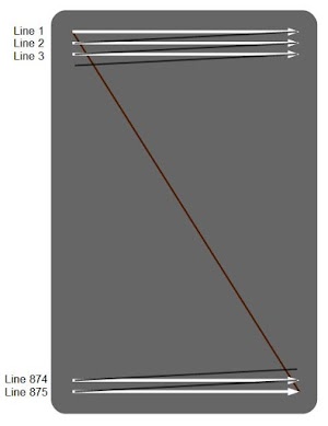
Since many readers may not be familiar with how CRTs work, I'll take a brief detour and explain how CRTs work. The cathode ray tube (CRT) ruled television displays from the 1930s until LCD displays took over about 10 years ago.2 In a CRT, an electron beam is shot at a phosphor-coated screen, causing a spot on the screen to light up. The beam scans across the screen, left to right and top to bottom in a raster pattern. The beam is turned on and off, generating a pattern of dots on the screen to form the image. The horizontal scan will turn out to be very important to this repair.

The Xerox Alto's display uses an 875-line raster scan. (For simplicity, I'm ignoring interlacing of the raster scan.)

The Xerox Alto's display uses an 875-line raster scan. (For simplicity, I'm ignoring interlacing of the raster scan.)

The cathode ray tube is a large vacuum tube containing multiple components, as shown below. A small electrical heater, similar to a light bulb filament, heats the cathode to about 1000°C. The cathode is an electrode that emits electrons when hot. A control grid surrounds the cathode; putting a negative voltage on the grid repels the negatively-charged electrons, reducing the beam strength and thus the brightness. The next grid has about 800 volts on it, attracting and accelerating the electrons. The focus grid, at about 600 volts, squeezes the electron beam to form a sharp spot. The anode is positively charged to a high voltage (17,000V), accelerating the electrons to hit the screen with high energy. The screen is coated with a phosphor, causing it to glow where hit by the electron beam. Finally, two electromagnets are arranged on the neck of the tube to deflect the beam horizontally and vertically in the raster scan pattern shown earlier; these are the deflection coils.

Diagram of a Cathode Ray Tube (CRT). Based on drawings by Interiot and Theresa Knott (CC BY-SA 3.0)

Diagram of a Cathode Ray Tube (CRT). Based on drawings by Interiot and Theresa Knott (CC BY-SA 3.0)

The photo below shows the Cathode Ray Tube (CRT) inside the Alto's monitor, with the screen at the right. In the center, the red deflection coils are mounted on the neck of the tube. The thick red wire provides 17,000 volts to the anode. This high voltage is generated by the flyback transformer, the UFO-like gray disk in the lower left.

Inside the Xerox Alto's display, the CRT picture tube is visible. The thick red wire provides 17,000 volts from the flyback transformer to the tube's anode. The other red wire is connected to the 500MΩ 6W bleeder resistor, the large white cylinder at the left. Note the dirt and debris on the flyback transformer from the system's storage in a barn.

Inside the Xerox Alto's display, the CRT picture tube is visible. The thick red wire provides 17,000 volts from the flyback transformer to the tube's anode. The other red wire is connected to the 500MΩ 6W bleeder resistor, the large white cylinder at the left. Note the dirt and debris on the flyback transformer from the system's storage in a barn.

Back to the broken display

Why would the display work for a moment, just as it is powered off? It must have something to do with voltage levels dropping as the power supplies shut down—something that wasn't working at full voltage, but worked at a lower voltage. One theory was that one of the CRT grids might have the wrong voltage. Since electrons are negative, they are attracted to positive voltages (such as the 17,000 volt anode) and repelled by negative voltages. If a grid was too negative, the electron beam could be blocked. Perhaps as the power supplies shut down, the negative grid problem briefly resolved itself.3

We opened up the display and measured some voltages, taking extreme care around the high voltages. Verifying the 17,000 V supply was easy; with a voltage this high, waving an oscilloscope probe a few inches away is sufficient to pick up a signal (below). The main 55V supply was also good. But when we checked the grid voltages, we didn't get anything.

The service manual shows the waveform you can pick up two inches away from the flyback transformer.

The service manual shows the waveform you can pick up two inches away from the flyback transformer.

The grid voltages and 17KV supply are generated by the flyback transformer. Since we saw the 17KV signal, we knew the horizontal deflection circuit and the flyback transformer were working. Perhaps a capacitor had failed, but we didn't find any bad ones. On the schematic we noticed a tiny lightbulb in the high-voltage circuit, an unexpected circuit element. We measured the bulb's resistance on the board (below) and found it was open. We figured the bulb must have burned out, but after removing it we discovered that instead one of the bulb's leads had broken off right at the glass case.

The bulb is visible in front of the right side of the transformer.

The bulb is visible in front of the right side of the transformer.

The service manual for the monitor called the bulb a "No. 1764." I was afraid that this was an internal part number and we wouldn't be able to determine the correct replacement bulb. However, Google revealed that this was a 28V 0.04A miniature bulb, sold by many vendors. Unfortunately we couldn't find any local stores that sold this bulb and we wanted to test out a fix immediately. So Marc performed some precision microscope soldering to reattach the broken wire. Since the wire had broken off right at the glass, reattaching it was very difficult but he succeeded. We re-installed the bulb and the display worked fine!

Why is there a bulb inside the power supply? I assume that it is used as a current limiter. Bulbs have very low resistance when cold, but increase resistance as they warm up. It seems crazy to subject a 28 V bulb to pulses of 600 volts, but since the pulses are only a few microseconds, the bulb survives them just fine.

The tiny bulb inside the display's power supply.

The tiny bulb inside the display's power supply.

Details on the power supply

The high-voltage power supply is described in the monitor service manual, but I'll give a brief summary here.4

The primary purpose of the horizontal sync circuit is to create a sawtooth current through the horizontal deflection coil to scan left-to-right across each row of the screen. A common trick in TVs is to use the high-frequency (26 kHz) horizontal sync to generate high voltages. To do this, the horizontal sync circuit sends high-current pulses (2-3 amps) through the flyback transformer. This step-up transformer produces the 17 kilovolts required by the CRT's anode. A second transformer winding produces -100 volts, while the third winding is used to generate 600V and 1000V. (Interestingly, cell phone chargers also use flyback transformers, but obviously at much lower voltages.)

The photo below shows the flyback transformer (left). The thick black wire at the bottom of the photo connects the 17KV from the transformer to the picture tube, while the colorful wires at the top provide the lower voltages.

Flyback transformer inside the monitor. The large white cylinder is a 500 megaohm, 6W resistor. You don't usually see such a high resistance combined with a high wattage, but the resistor bleeds off the high voltage from the CRT.

Flyback transformer inside the monitor. The large white cylinder is a 500 megaohm, 6W resistor. You don't usually see such a high resistance combined with a high wattage, but the resistor bleeds off the high voltage from the CRT.

The schematic below indicates the key components of the power supply. The switching transistor is driven by the horizontal sync input. When it switches on, current (red line) builds up in the flyback transformer, storing energy in the transformer's magnetic field. When the transistor switches off, this stored energy is released into the secondary windings, producing 17KV for the anode and -100V for the brightness grid. In addition, a 600V pulse is created across the primary. The pulse (yellow line) flows through the bulb and a diode, generating 600V for the focus grid. The voltage doubler circuit (circled in pink) generates 1000V for the second (accelerator) grid.

The high-voltage power supply is driven by the horizontal deflection circuit.
The switching transistor puts 55 volts across the flyback transformer. When it switches off, the flyback transformer produces 17 kilovolts for the CRT anode, as well as powering the 600V, 1000V and -100V supplies.

The high-voltage power supply is driven by the horizontal deflection circuit. The switching transistor puts 55 volts across the flyback transformer. When it switches off, the flyback transformer produces 17 kilovolts for the CRT anode, as well as powering the 600V, 1000V and -100V supplies.

Why did the display originally show a picture for a moment as it was powered off? With the bulb not working, the 800V acceleration grid and the focus grid didn't receive any voltage, but the brightness grid was still powered (since -100V comes from a different winding). My theory is that without the attraction from the acceleration grid, electrons couldn't get past the negative brightness grid. But when the brightness grid lost power, the electron beam was no longer blocked and could reach the screen, until everything else shut down moments later.

Conclusion

Cathode ray tubes were the dominant display technology until LCD displays took over about 10 years ago. Now, CRT TV repair is a retro activity, involving circuits such as horizontal deflection, video amplifiers, and high-voltage flyback transformers that were formerly well-known but are now more obscure.

We tracked down the display's problem to a tiny light bulb, an unusual component to find in a critical role in a high-voltage power supply. Surprisingly, despite being exposed to 600 volt pulses, the problem with this 28 volt bulb wasn't that it had burnt out, but that one of its tiny leads had broken. After repairing the bulb, the display worked fine. Unlike our previous display which had a very faint CRT, this one produced a crisp, bright image. Since we got the display working and didn't get any high-voltage shocks, I consider this a successful restoration session.

The repaired display shows a test pattern, generated by the crttest program. The screen is bright and sharp, but the horizontal centering still needed adjustment.

The repaired display shows a test pattern, generated by the crttest program. The screen is bright and sharp, but the horizontal centering still needed adjustment.

Thanks to the Living Computer Museums + Lab for providing the display test board. Thanks to Al Kossow and Bitsavers for the scanned service manual.

Notes and references

  1. For more on the Alto's monitor, see my article from last year about restoring our first display

  2. A computer monitor is essentially a television set, but without the tuner to select the desired channel from the antenna. In addition, televisions have circuitry to extract the horizontal sync, vertical sync and video signals from the combined broadcast signal. These three signals are supplied to the Alto monitor separately, simplifying the circuitry. 

  3. I should admit that Marc and Carl had the right theory about the problem. My theory that the video input voltage might be too high didn't pan out. 

  4. I didn't discuss the 55V supply that powers the monitor. It is a straightforward regulated linear power supply driven from the 120V AC input. I also also didn't explain how the horizontal deflection coil operates. it is driven by the same transistor as the flyback transformer, but uses a fairly complex inductor-capacitor resonance circuit to generate the scan across the screen. (The scan current is a sawtooth; a smooth scan left-to-right followed by a rapid retrace back to the left.) For a thorough discussion of how the display's power supply works, see page 3-4 of the service manual

  5. The 7-wire interface used a 15-wire cable with standard DB-15 (serial port) connectors. It sent seven ECL signals as differential pairs, and used the remaining wire for ground. Calling it "7-wire" seems a bit misleading, since it used 15 wires in total. The board schematic is in the Dorado schematics page 159. The video signal was multiplexed across four of the signals; this reduced the bandwidth requirement by a factor of four. One signal was serial data; this transmitted the keyboard and mouse information. The remaining two signals were (apparently redundant) clocks. The protocol supported daisy-chaining, so multiple peripherals (such as a printer) could be connected.

    This 7-wire Terminal Interface board was used by Xerox PARC to connect a keyboard/display/mouse to a remote Dorado minicomputer

    This 7-wire Terminal Interface board was used by Xerox PARC to connect a keyboard/display/mouse to a remote Dorado minicomputer

    The photo above shows the 7-wire terminal interface board inside the display. The large chips in the upper right are the 6532"RIOT" I/O chip, the 6502 microprocessor, and a 2716 EPROM holding the code. The remaining chips are a mixture of TTL and ECL. At the bottom are connectors for 7-wire in, 7-wire out, and the keyboard. The connector to the monitor itself is in the upper center. 

The Xerox Alto, Smalltalk, and rewriting a running GUI

$
0
0
Be sure to read the comment from Alan Kay at the bottom of the article!

We succeeded in running the Smalltalk-76 language on our vintage Xerox Alto; this blog post gives a quick overview of the Smalltalk environment. One unusual feature of Smalltalk is you can view and modify the system's code while the system is running. I demonstrate this by modifying the scrollbar code on a running system.

Smalltalk is a highly-influential programming language and environment that introduced the term "object-oriented programming" and was the ancestor of modern object-oriented languages.1 The Alto's Smalltalk environment is also notable for its creation of the graphical user interface with the desktop metaphor, icons, scrollbars, overlapping windows, popup menus and so forth. When Steve Jobs famously visited Xerox PARC, the Smalltalk GUI inspired him on how the Lisa and Macintosh should work.2

Our Xerox Alto running Smalltalk-76.

Our Xerox Alto running Smalltalk-76.

The Alto was a revolutionary computer designed at Xerox PARC in 1973 to investigate personal computing. It introduced the GUI, high-resolution bitmapped displays, WYSIWYG editors, Ethernet, the optical mouse and laser printers to the world, among other things. I've been restoring an Alto from YCombinator, along with Marc Verdiell, Carl Claunch My full set of Alto posts is here and Marc's extensive videos of the restoration are here.

The desktop

Smalltalk introduced the desktop metaphor used in modern computing.3 It included overlapping windows4, multiple desktops and pop-up menus. These windows could be moved and resized with the mouse. (The biggest missing desktop feature was desktop icons, which Xerox later introduced in the Star computer.) To understand how revolutionary this was, consider that the Apple 1 microcomputer came out in 1976, displaying 24 lines of 40 uppercase characters. The mainframe and minicomputer worlds were focused around punched cards, line printers, Teletypes, and dumb CRT terminals. Alan Kay changed all this with his vision of a computer desktop with windows that could be directly manipulated, windows containing fancy typography or images.

Smalltalk introduced the desktop environment, with overlapping windows for multiple applications.

Smalltalk introduced the desktop environment, with overlapping windows for multiple applications.

The screenshot above shows the Smalltalk-76 desktop. At the bottom, a drawing program displays the Smalltalk elf image.5 Icons allow selection of drawing mode, line style, brush color (grayscale), and so forth. The Smalltalk class browser is in the middle. In the upper right is a file viewer. Finally, in the upper left is a window for entering Smalltalk statements, essentially a shell or REPL.

Dynamically changing the running system

One of the most interesting things about the Smalltalk environment is that all the Smalltalk code can be examined and modified, even while the system is running. The class browser below lets you select (using the mouse) a functional area such as "Basic Data Structures" or "Files". You can then select a class in that area, functionality within the class, and then a particular method. The browser then displays the code running on the system. All the Smalltalk code can be examined in this way, making the system's implementation very transparent.

Using the Smalltalk class browser, we can view the code to show a ScrollBar.

Using the Smalltalk class browser, we can view the code to show a ScrollBar.

In the screenshot above, I use the class browser to access "Panes and Menus", then "ScrollBar", then "Image" and finally "show". This displays the code for the scrollbar's "show" method, which draws the scrollbar. This code draws a black rectangle, and then insets a white rectangle, resulting in a black-bordered rectangle for the scrollbar. (Note the unusual dotted-circle character ☉ that Smalltalk-76 uses to create a Point from two Numbers.)

The unusual feature of the class browser is that you can use it to change the system's code, while the system is running, and everything will pick up the new code. For example, I can change how scrollbars are drawn. In the screenshot below, I changed clear: white to clear: black. Pressing the middle mouse button pops up a menu, and I can select "compile". This causes the scrollbar code to be recompiled—while the system is still running. (Note the modern appearance of the contextual pop-up menu.)

After changing the code, I selected "compile" from the pop-up menu.

After changing the code, I selected "compile" from the pop-up menu.

The result of this change is that all scrollbars (for existing or new windows) will now have a black background, as you can see below. The key point is this change was made while the system was running; there is no need to restart anything. Even existing windows get the new scrollbars.

Scrollbars now appear with a black background, even for existing windows.

Scrollbars now appear with a black background, even for existing windows.

Although this scrollbar change was rather trivial, major changes can be made to the running Smalltalk system. One well-known story of changing Smalltalk's behavior on the fly is from Steve Jobs' visit to Xerox PARC. Steve Jobs didn't like the way the window scrolled line-by-line, so Smalltalk implementer Dan Ingalls rewrote the scrolling code in a minute and implemented smooth scrolling while the system was running, much to Jobs' surprise.6

A closer look at some Smalltalk code

In Smalltalk, even most of the math functions are written in Smalltalk. For instance, suppose we wonder how square roots are computed. We can look at the square root function in the class browser by going to "Numbers", "Float", "Math functions", "sqrt". This brings up the seven lines of code below for the square root function. We can see that the code uses five iterations of Newton's method to approximate the square root.

Looking at the square root code in the Smalltalk-76 class browser.

Looking at the square root code in the Smalltalk-76 class browser.

If you're used to Java or C++, this object-oriented code may look strange, especially since Smalltalk uses some strange characters. The first line of code above defines local variables guess and i. In the next line, the right arrow ⇒ implements an "if" statement. If the number receiving the square root message (self) is 0, then 0 is returned (via the up arrow ⇑ return symbol) and if it is negative an exception is raised. The square brackets define blocks, similar to curly braces in C. The instfield line is a bit tricky; it pulls the exponent out of the floating point number and divides it by 2, yielding a reasonable starting point for the square root. Finally, the for loop applies Newton's method 5 times and returns the result. Note the unusual double colon symbol ⦂; this delays evaluation of the argument, so it can be evaluated multiple times in the loop.7

You might think that executing Smalltalk code for math operations would be very slow, and that is the case. The good news is that basic operations such as addition are implemented with short cuts, rather than full message passing. But other operations are slow; the team described performance as between "majestic" and "glacial". Xerox PARC ended up creating the Dorado, a much faster minicomputer than the Alto, to improve performance.

Conclusion

Although Smalltalk wasn't the first object-oriented programming language, Smalltalk introduced the term object-oriented programming and was very influential in later object-oriented programming languages. Most modern object-oriented languages, from Objective-C and Go to Java and Python, show the influence of Smalltalk. Smalltalk was also responsible for design patterns. The famous "Gang of Four"Design Patterns book describes design patterns in Smalltalk and C++.8

Smalltalk systems are still in use. Smalltalk-76 (and the earlier 71 and 72 versions) were intended for research, but Xerox released the Smalltalk-80 version; it was licensed by Xerox to HP, Apple, Tektronix and DEC for royalty-free distribution. Smalltalk-80 in turn led to modern Smalltalk systems such as Pharo, GNU Smalltalk and Squeak (which led to the Scratch language for children).

If you want to try Alto Smalltalk out for yourself, you can use the Contralto emulator, built by the Living Computers Museum. I explain how to run it here. (Most of the screenshots above are from Contralto rather than the live Alto, for clearer images.) Be warned, however, that Smalltalk on the Alto (live or emulated) is painfully slow.

Notes and references

  1. Smalltalk was developed on the Xerox Alto by Alan Kay, Dan Ingalls, Adele Goldberg and others. 

  2. The details of Steve Jobs' visits to Xerox PARC are highly controversial but the description in Dealers of Lightning seems most accurate. 

  3. Englebart's Mother of All Demos was fundamental to the development of the GUI, introducing the mouse and windows, among other things. This demo had a large influence on Xerox PARC. 

  4. For performance reasons, only the foreground window was active and background windows were not redrawn. 

  5. Screenshots of Smalltalk-76 very often include the lute-playing elf image, so I tracked down the image and figured out how to display it. The command is BitRect new fromuser; filin: 'elf'; edit. This creates a new BitRect object and gets the dimensions from the user. Then it sends a filin: 'elf' message to the BitRect, which performs file input from the elf.pic file. Finally, an edit message is sent to the BitRect, causing it to be opened in the image editor. 

  6. For details on Dan Ingalls' live implementation of smooth scrolling in Smalltalk-78, see this page. The story is also in Dealers of Lightning, page 341. (Dealers of Lightning is the best book I've come across describing Xerox PARC and the development of the Alto.) 

  7. If you want more information on Smalltalk-76, The Smalltalk-76 Programming System Design and Implementation provides a good overview. The document How to use the Smalltalk-76 system gives details on running Smalltalk on the Alto. Unfortunately, the special characters don't appear, making the document slightly cryptic. See Alan Kay's The Early History of Smalltalk for a detailed discussion of Smalltalk's background and history. 

  8. People often think of design patterns as a Java thing, but the Design Patterns book was published in 1994, prior to Java's release in 1995. The original design patterns referred to C++ and Smalltalk. 

Steve Jobs, the Xerox Alto, and computer typography

$
0
0

Steve Jobs gave an inspirational commencement address at Stanford in 2005. He described how his decision to drop out of college unexpectedly benefitted the Macintosh years later:

Reed College at that time offered perhaps the best calligraphy instruction in the country. [...] Because I had dropped out and didn’t have to take the normal classes, I decided to take a calligraphy class to learn how to do this. I learned about serif and sans serif typefaces, about varying the amount of space between different letter combinations, about what makes great typography great. It was beautiful, historical, artistically subtle in a way that science can’t capture, and I found it fascinating.

None of this had even a hope of any practical application in my life. But 10 years later, when we were designing the first Macintosh computer, it all came back to me. And we designed it all into the Mac. It was the first computer with beautiful typography. If I had never dropped in on that single course in college, the Mac would have never had multiple typefaces or proportionally spaced fonts. And since Windows just copied the Mac, it’s likely that no personal computer would have them. If I had never dropped out, I would have never dropped in on this calligraphy class, and personal computers might not have the wonderful typography that they do.

While this is an uplifting story about trusting in destiny, the real source of this computerized "wonderful typography" is the Xerox Alto computer, built by Xerox PARC in 1973. The Alto was a revolutionary system, one of the first to use a high-resolution bitmapped display, a GUI, and an optical mouse. The first WYSIWYG (What You See Is What You Get) text editor was created at Xerox PARC in 1974 by Charles Simonyi, Butler Lampson and other Xerox researchers. The Alto system supported many high-quality fonts, including proportionally spaced fonts with ligatures.1 Xerox PARC also invented the laser printer in 1971, allowing high-resolution documents to be printed.2

The Xerox Alto displaying Steve Job's commencement speech with fancy formatting in the Bravo editor. That's an old Macintosh 512K in the background.

The Xerox Alto displaying Steve Job's commencement speech with fancy formatting in the Bravo editor. That's an old Macintosh 512K in the background.

Xerox PARC used this software for its Alto documentation, producing high-quality printed manuals that mixed text and computer-generated drawings. The Alto User's Handbook (below), for example, combined nicely-formatted text with computer-generated drawings.6 Thus, by the time Steve Jobs founded Apple in 1976, Xerox had created a high-quality desktop publishing system. Steve Jobs' claim that the Mac (1984) was the first computer with beautiful typography is wrong by about a decade.

The Alto User's Handbook was created using the Alto's desktop publishing software, including Bravo and Draw. The closeup on the right shows how typography was combined with drawings.

The Alto User's Handbook was created using the Alto's desktop publishing software, including Bravo and Draw. The closeup on the right shows how typography was combined with drawings.

Steve Jobs famously visited Xerox PARC in 1979 and saw Xerox's GUI technology. The revolutionary systems he saw there inspired the direction for the Lisa and Macintosh. (This led Xerox to attempt to sue Apple in 1989 for copying its technology.) 5 Jobs later said about Xerox's GUI: "I thought it was the best thing I’d ever seen in my life. [...] And within – you know – ten minutes it was obvious to me that all computers would work like this some day." So although Steve Jobs claimed in his commencement speech, "If I had never dropped in on that single course in college, the Mac would have never had multiple typefaces or proportionally spaced fonts", the Xerox PARC visit appears to be the real source.7

Closeup of Steve Jobs' commencement speech in the Bravo editor on the Xerox Alto. This shows a few of the proportionally-spaced fonts available on the Alto. It also demonstrates centered and  justified text.

Closeup of Steve Jobs' commencement speech in the Bravo editor on the Xerox Alto. This shows a few of the proportionally-spaced fonts available on the Alto. It also demonstrates centered and justified text.

In his commencement address, Steve Jobs also claimed, "And since Windows just copied the Mac, it's likely that no personal computer would have [multiple typefaces or proportionally spaced fonts]." The ironic thing is that Microsoft Word was developed by Charles Simonyi, the same Simonyi who co-wrote Xerox's Bravo editor in 1973. Since the Macintosh came out in 1984, the accusation of copying is directed the wrong way. It's also absurd to claim that no other personal computer would have these features without Jobs, since the Alto had them years earlier.4

Conclusion

While Steve Job's commencement speech is inspiring, it is also an example of the "reality distortion field" at work. While he claimed that a calligraphy course at Reed inspired him to provide typography support in the Macintosh, the Xerox Alto and Jobs' visit to Xerox PARC in 1979 are surely more important. The Macintosh owes everything from the WYSIWYG editor and spline-based fonts to the bitmapped display and laser printer to the Xerox Alto. Of course, Steve Jobs deserves great credit for making desktop publishing common and affordable with the Macintosh and the LaserWriter, something Xerox failed to do with the Xerox Star, an expensive ($75,000) system that commercialized the Alto's technology.

I've been restoring an Alto from YCombinator, along with Marc Verdiell, Carl Claunch and Luca Severini. My full set of Alto posts is here and Marc's extensive videos of the restoration are here. You can follow me on Twitter here for updates on the restoration.

Notes and references

  1. The Alto supported high-quality spline-based fonts, as well as bitmap fonts. PARC built an interactive font editor (FRED) and an interactive rasterizer (PREPRESS). This system is essentially an ancestor of the TrueType fonts used today (details). 

  2. Xerox PARC also invented Press, a device-independent printer file format that eventually led to PDF files. First, Xerox's Press format led to the Interpress product. Two of Interpress's creators left Xerox and started Adobe, where they created the PostScript page definition language. The ubiquitous PDF format is in turn a descendant of PostScript. Some history on Xerox's early printers and Press format is here

  3. In 1975, Xerox PARC developed an improved modeless version of the Bravo editor for use by textbook publisher Ginn & Co., which used this system for the majority of their books. This illustrates that Xerox's desktop publishing was used commercially, not just for research. See Fumbling the Future, Chapter 9 for details. The document Gypsy Evaluation is Xerox's 1976 evaluation of the system. 

  4. While the term "personal computer" is vague, it's clear that the Alto's builders intended it as a personal computer. See for example Alto: A personal computer, Alto: A Personal Computer System Hardware Manual and The Xerox Alto Computer which describes the Alto as a "personal computer to be used for research". 

  5. The details of Steve Jobs' visits to Xerox PARC are highly controversial but the description in Dealers of Lightning seems most accurate. It's well known that as part of Xerox investing in Apple, Steve Jobs arranged to see demos of the PARC technology. However, this didn't include licensing of the technology. 

  6. Examples of documents created with the Xerox Alto are the hardware manual, Alto User's Handbook, and Alto Newsletter

  7. Note that the popular Apple II computer (1977) didn't have beautiful typography or multiple fonts—it didn't even include lower case characters. Lower case support was finally added to the Apple IIe in 1983. 

Identifying the "Early IBM Computer" in a Twitter photo: a 405 Accounting Machine

$
0
0

The photo below of a "woman wiring an early IBM computer" has appeared on Twitter a bunchoftimes, and it stoked my curiosity: what was the machine in the photo? Was it really an early IBM computer? I was a bit skeptical since the machine in the photo is much smaller than IBM's first room-filling computers, and there aren't any vacuum tubes visible. I investigated this machine and it turned out to be not a computer, but an IBM 405 "Alphabetic Accounting Machine" from 1934, back in the almost forgotten pre-computer age of tabulating machines.1

A common photo on Twitter shows a woman wiring an early IBM computer.

A common photo on Twitter shows a woman wiring an early IBM computer.

The image is from photographer Berenice Abbott who took many scientific photographs from 1939 to 1958. She photographed everything from basic magnetic field and optics experiments to research on early television tubes, and many of these photos were used in physics textbooks. Her photos (including IBM photos) were published in the book Documenting Science. I had hoped that the book would identify the computer in the photo, but it merely said "IBM Laboratory: Wiring an early IBM computer". Surprisingly for an art book, it didn't even give a date for the photo.

The diagram below shows the back view of an IBM 403 accounting machine, which IBM introduced in 1948.2 (An accounting machine (also called a tabulator) summed up and printed records from punched cards for applications such as payroll or inventory.) Note the similarities with the Abbott photo: the thick laced wire bundles, the vertical wire bundles in the middle for the counters, and the hinged doors that swing open.

Back view of an IBM 403 accounting machine. From the IBM 402/403 Field Engineering Manual.

Back view of an IBM 403 accounting machine. From the IBM 402/403 Field Engineering Manual.

A second Berenice Abbott photo shows the machine from a slightly different angle.3 The "Card Feed Circuit Breaker Unit" in the upper right looks like a perfect match between the IBM 403 and the Abbott photo. The dangling cables from the counters in the middle look right, as well as the thick cable between the counters and the circuit breaker unit. The 403 diagram above shows a large printing carriage on top, while the Abbott photo just shows a base, presumably because the carriage hadn't been installed yet.

A second photo of "Woman wiring an early IBM computer" by Berenice Abbott.

A second photo of "Woman wiring an early IBM computer" by Berenice Abbott.

Although the machine in the Abbott photo looks very similar to the IBM 403, there are a few differences if you look carefully. One clear difference is the IBM 403 had caster wheels attached directly to the frame, while the machine in the photos has stubby curved legs. In addition, the doors of the IBM 403 were hinged at a different place. In the Abbott photos, the doors are attached just to the left of the counters and to the right of the card feed circuit breaker unit. But the IBM 403 has some bulky components to the left of the counters such as the "Bijur pump" (an oil pump), and components on the right such as the drive motor. Overall, the machine in the Abbott photos has a narrower cabinet than the IBM 403. Additionally, the thick cable snaking down between the IBM 403's circuit breaker units appears to go straight down in the photos. Thus, although the machine in the photos is very similar to the IBM 403, it's not an exact match.

After more research into IBM's various accounting machines, I conclude that machine in the photos is the IBM 405, an IBM accounting machine introduced in 1934 (earlier than that 1948 IBM 403 despite the larger model number).4 The IBM 405 (below) had curved legs that match the Abbott photos. In addition, the 405 has a narrower main cabinet than the 403, with bulky additional components attached to the left and right, outside the legs. This matches the narrower cabinet in the Abbott photos. (The 403 was an improved and modernized 405, explaining the overall similarity between the two machines.)

An IBM 405 accounting machine. Photo courtesy of Columbia University Computing History.

An IBM 405 accounting machine. Photo courtesy of Columbia University Computing History.

Punched cards were a key part of data processing from 1890 until the 1970s, used for accounting, inventory, payroll and many other tasks. Typically, each 80-column punched card held one record, with data stored in fixed fields on the card. The diagram below shows a typical card with columns divided into fields such as date, vendor number, order number and amount. An accounting machine would process these cards: totaling the amounts, and generating a report with subtotals by account and department, as shown below.

Example of a punched card holding a 'unit record', and a report generated from these cards. The accounting machine can group records based on a field to produce subtotals, intermediate totals, and totals. From Manual of Operation.

Example of a punched card holding a 'unit record', and a report generated from these cards. The accounting machine can group records based on a field to produce subtotals, intermediate totals, and totals. From Manual of Operation.

Punched-card data processing was invented by Herman Hollerith for the 1890 US census, which used a simple tabulating machine to count census data, stored on punched cards. Tabulating machines steadily became more complex, becoming feature-laden "accounting machines" that could generate business reports. Businesses made heavy use of these electromechanical accounting machines and by 1944, IBM had 10,000 tabulating and accounting machines in the field.

Accounting machines were "programmed" with a removable plugboard. By switching the plugboard, an accounting machine could be rapidly reconfigured for different tasks. Each wire corresponded to one character or digit. Wires plugged into the plugboard connected columns on the input card to adders. Each column on the printer had an associated wire controlling what got printed. Other wires had control functions. (I explained the tax preparation plugboard below in detail in this article.)

Plugboard to generate a tax report on an IBM 403 accounting machine. Courtesy of Carl Claunch.

Plugboard to generate a tax report on an IBM 403 accounting machine. Courtesy of Carl Claunch.

The IBM 405 was IBM's first "Alphabetic Accounting Machine," able to print text as well as numbers. It had more complexity than you might expect from the 1930s, able to generate three levels of subtotals, intermediate totals, and grand totals. It could process up to 150 cards per minute; that's remarkably fast for an electromechanical system, reading and summing more than 2 cards per second. The 405 was IBM's flagship product for many years, with IBM manufacturing 1500 of them per year. Like most IBM machines, the 405 was usually rented rather than purchased; it cost over $1000 a month (equivalent to about $15,000 per month in 2017 dollars). Renting out these machines (and selling the punch cards) was highly profitable for IBM, with the IBM 405 accounting machine called "the most lucrative of all IBM's mechanical glories".5

Amazingly, although accounting machines were designed for business purposes, they were also used for scientific computation in the 1930s and 1940s, before digital computers existed. They solved everything from differential equations and astronomy computations to nuclear bomb simulations for the Manhattan Project.6

How does an accounting machine work and what are all those parts?

Accounting machines (also called tabulators) were built from electromechanical components, rather than transistors or even vacuum tubes. The main components in accounting machines were electromechanical counters and relays. Everything was synchronized to rotating driveshafts that ran the counters, card reader and printer. In a way, accounting machines were more like cars than computers, with a motor, clutches, driveshafts, an oil pump, gears and cams.

Counters

The heart of the accounting machine was the mechanical counter, a digit wheel somewhat like an odometer. Each wheel stored one digit, with the value indicated by the rotational position of the wheel. To add a number, say 3, to the counter, a clutch was briefly activated, causing the drifeshaft to rotate the counter three more positions. Since these counters were adding 2 1/2 numbers per second, they were spinning rapidly with the clutches engaging and disengaging with precision timing. By combining multiple counters, numbers of up to 8 digits could be handled. The counter kept a running total of the numbers fed into it. Since it accumulated these numbers, the counter was known as an accumulator, a term still used in computing.

A counter unit from an IBM accounting machine. The two wheels held two digits. The electromagnets (white) engaged and disengaged the clutch so the wheel would advance the desired number of positions.

A counter unit from an IBM accounting machine. The two wheels held two digits. The electromagnets (white) engaged and disengaged the clutch so the wheel would advance the desired number of positions.

The photo above shows a board with two counters: the two wheels on the left stored two digits. The counters are more complex than you might expect, with electromechanical circuits to handle carries (including fast carry lookahead). The clutch is underneath the wheel and is engaged by the metal levers in the photo, controlled by electromagnets. A gear underneath the clutch connects the counter to the driveshaft. The electrical connections on the right control the clutch and allow the values from the counters to be read out. Since the IBM 405 had 16 accumulators, with up to 8 digits, many counters were required, resulting in the mass of counter wires in the photos.

Relays

Another key component of the accounting machine was the relay, an electromagnetic switch. The control logic of the accounting machine was implemented with hundreds of relays, which would turn on and off to direct the various components of the accounting machine. Example relay functions are switching on when punched cards are in the input hopper, selecting addition or subtraction for a counter, generating the final total when all cards are done, or printing a credit symbol for a negative balance.

The back of the IBM 403 accounting machine shows numerous relays, used to control the machine.

The back of the IBM 403 accounting machine shows numerous relays, used to control the machine.

The relays were mounted on swing-out panels. The photo above shows an IBM 403 with the panels closed. In the Abbott photos the relay panels are opened and you can see the extensive wiring that connected the relays to the rest of the system.

Circuit breakers

The final component I'll explain is the "circuit breaker," which has nothing to do with the circuit breakers in your house. Instead, these are cam-controlled switches that turned on and off (breaking circuits) as the drive shafts rotated. Dozens of circuit breakers provided the timing signals to the accounting machine, ensuring all operations in the machine were synchronized to the drive shaft. (Every 18° of drive shaft rotation corresponded to reading one row on a punched card, moving one character position on a printer typebar, or advancing a counter wheel by one position.)

Conclusion

The woman in Abbott's photos illustrates the large, but mostly ignored role that women played in electrical manufacturing. Women formed the majority of workers in the 1920s radio manufacturing industry, and their presence in electrical manufacturing increased even more when World War II led many women to take industrial jobs. The famous ENIAC computer (1946) also illustrates this: most of the "wiremen" assembling the ENIAC computer were in fact women, probably recruited from the telephone company or radio assembly.8

The photos also provide a glimpse into the era before digital computers, when businesses used electromechanical accounting machines and tabulators for their data processing. Although you'd expect a machine from 1934 to be primitive, the IBM 405 accounting machine in the photos was an advanced piece of technology for its time, containing 55,000 parts and 75 miles of wire.5 These punched card machines were also capable of performing complex scientific tasks, even contributing to the Manhattan Project. In the 1960s, businesses gradually switched from accounting machines to stored-program business computers such as the IBM 1401. Even so, IBM continued marketing accounting machines until 1976.

Follow me on Twitter or RSS to find out about my latest blog posts.

Notes and references

  1. By the "era before computers", I mean before digital electronic computers came along in the 1940s. There's a long history of computing machines, analog computers, and human computers (as shown in Hidden Figures) before digital computers came along. Two interesting books that cover this history are The First Computers—History and Architecture or The Computer: From Pascal to von Neumann

  2. IBM's 402 and 403 accounting machines were the same except the 403 could print three-line addresses. This feature was called MLP (multi-line printing) and was useful for printing addresses on invoices, for instance. So when I refer to the IBM 403 accounting machine, I'm also including the IBM 402. 

  3. I was surprised to realize that there are two different, but nearly identical photos of the woman wiring the IBM machine floating around. In first photo, the woman's right leg is straight, there's a screwdriver in front of the bench and she's wiring the left side of the machine. In the second, the woman's left leg is straight and she's wiring the middle of the machine. 

  4. I couldn't find any manuals for the IBM 405 or photos of the back of a 405, so I can't totally nail down the identification. There's a possibility that the Abbott photos show an IBM 401 accounting machine (below), which was similar to the 405 but introduced a year earlier. The IBM 401 and IBM 405 both had the same basic shape and arrangement of components. The main difference is 405 had a full cabinet in front while the 401 was empty in the front with a bar bracing the front feet. The Abbott photos seem to show a full cabinet like the 405, rather than the open 401. Also, since the 405 was a much more popular machine than the 401—the 405 was the "flagship of IBM's product line until after World War II"—the photos are most likely the 405.

    IBM 401 accounting machine (1933). Photo courtesy of Computer History Museum.

    IBM 401 accounting machine (1933). Photo courtesy of Computer History Museum.
  5. While I couldn't find detailed manuals for the IBM 405, several sources provide information. One source is Computing before Computers (online) p144. IBM has a FAQ with a short overview. Columbia's Computer History page on the 405 has a longer discussion. Also see IBM's Early Computers, pages 18-22 for information on the IBM 405. Computer: Bit Slices from a Life has some hands-on stories of the IBM 405 (online). Computer: A history of the information machine page 51 has some information on the IBM 405. 

  6. See Punched Card Methods in Scientific Computation, 1940 for details on how accounting machines were used for scientific computation. The book is by W. J. Eckert, confusingly unrelated to the ENIAC's J. Presper Eckert. The use of IBM accounting machine by the Manhattan Project is described by Feynman in Los Alamos from Below, p25; and in this page. The Manhattan Project used a 402 accounting machine, several IBM 601 multiplying punches for multiplication, and other card equipment (reference, with more details in Early Computing at Los Alamos). 

  7. I was unable to find documentation on the IBM 405 specifically, but Bitsavers has manuals for the later 402/403 accounting machines. The operation of accounting machines is discussed in detail in IBM 402, 403 and 419 Accounting Machines: Manual of Operation. For a thorough discussion of how the machine works internally, see IBM 402, 403, 419 Field Engineering Manual of Instruction. For an overview of how plugboard wiring for IBM's works, see IBM Functional Wiring Principles

  8. Women and Electrical and Electronics Manufacturing provides a detailed discussion of the history of women in technological manufacturing in the 20th century. The book ENIAC in Action describes how most of the wiring of the ENIAC was done by women. It also has a detailed discussion of the role of women as programmers for early computers such as the ENIAC. 


Fixing the Ethernet board from a vintage Xerox Alto

$
0
0

A Xerox Alto system on the East coast had Ethernet problems, so the owner sent me the Ethernet board to diagnose. (After restoring our Alto, we've heard from a couple other Alto owners and try to help them out.) This blog post describes how I repaired the board and explains a bit about how the Alto's groundbreaking Ethernet worked.

The Alto was a revolutionary computer designed at Xerox PARC in 1973, introducing the GUI, high-resolution bitmapped displays and laser printers to the world. But one of its most important contributions was Ethernet, the local area network that is still heavily used today. While modern Ethernets handle up to 100 gigabits per second, the Alto's Ethernet was much slower, just 3 megabits per second over coaxial cable. Even so, the Alto used the Ethernet for file servers, email, network boot, distributed games and even voice over Ethernet.

An extender board made it easy to probe the Ethernet card in the Xerox Alto. The chassis is pulled out to access the boards.  Above the chassis is the disk drive, which stores just 2.5 megabytes on a 14-inch disk pack.

An extender board made it easy to probe the Ethernet card in the Xerox Alto. The chassis is pulled out to access the boards. Above the chassis is the disk drive, which stores just 2.5 megabytes on a 14-inch disk pack.

The Alto's chassis slides out of the cabinet, allowing access to the circuit boards (see above). To test the Ethernet board, I plugged it into the Alto we've restored. The Ethernet board is hanging out the right side of the chassis because I used an extender board.

The board had a couple straightforward problems—a chip with a bent pin (which I straightened) and another chip with broken pins. (While some people recommend re-seating chips on old boards, this can create new problems.) The broken chip was a 74S86, a quadruple XOR gate that has been obsolete for years (if not decades). I replaced it with a 74LS86, a similar but non-obsolete chip.1

When I powered up the Alto, I didn't get anything from the Ethernet board: it was not sending or receiving successfully. This double failure was a bit surprising since malfunctions usually affect just one direction. But I quickly discovered a trivial problem: when I pulled out the Alto's cabinet to access the circuit boards, the Ethernet connector on the back came loose. After plugging the connector in, I saw that the Alto was sending packets successfully, but still wasn't receiving anything.

Oscilloscope trace from the Ethernet board. Yellow is input data, green is R-C filtered, blue is detected edges. The blue trace is a bit of a mess with runt pulses.

Oscilloscope trace from the Ethernet board. Yellow is input data, green is R-C filtered, blue is detected edges. The blue trace is a bit of a mess with runt pulses.

I started probing the Ethernet board's input circuit with the oscilloscope. The board was receiving the input okay, but a few gates later the signals looked kind of sketchy, as you can see above. The yellow trace is the input Ethernet signal. The board applies an R-C filter (green) and then the signal edges are detected (blue). While the input (yellow) is a clean signal, the green signals only go up to about 2 volts, not the expected 4-5 volts. Even worse, the blue waveform is irregular and has "runt" pulses—short irregular signals that don't go all the way up. With waveforms like this, the board wouldn't be able to process the input.

Manchester encoding and the decoding circuit

I'll take a detour to explain the Ethernet's Manchester encoding, before getting into the details of the circuitry.

The Alto's Ethernet encoded data over the coaxial cable using Manchester encoding.32 In this encoding, a 1 bit is sent as a 1 followed by a 0, while a 0 bit is sent as a 0 followed by a 1. The diagram below shows how the bits "0110" would be encoded. A key reason to use this encoding is that simplifies timing on the receiver, since it is self-clocking. Note that there is a transition in the middle of each cell that can be used as a clock. (The obvious scheme of just sending the bits directly has the problem that in a long string of 0's, it's hard to know exactly how many were transmitted.)

An example of Manchester encoding, for the bits 0110.

An example of Manchester encoding, for the bits 0110.

To decode the Ethernet signal arriving at the Alto, the first step is to extract the clock signal that indicates the timing of the bits. To extract the clock, the transitions in the middle of each bit cell must be detected. The trick is to ignore transitions at the edges of cells. The diagram below shows how the clock is extracted. First, edge pulses are generated for each transition edge of the input. Then, a clock pulse is generated for each edge pulse. The clock pulse about 75% of the width of the bit cell, and any second pulse that happens while the clock is still high is blocked. (The edge circled in red is an example of an ignored edge.) The result is the steady clock signal, synchronized to the input.4 This clock is used to latch the input signal value into a shift register, which converts the serial Ethernet stream into a word value usable by the Alto.

Extracting the clock signal from a Manchester-encoded Ethernet input. Edges are extracted from the input signal and used to trigger the clock. An edge too close to the previous (red) is dropped.

Extracting the clock signal from a Manchester-encoded Ethernet input. Edges are extracted from the input signal and used to trigger the clock. An edge too close to the previous (red) is dropped.

The schematic5 below shows the circuit that performs this clock extraction. There are a few tricks in this interesting semi-analog circuit. When the Ethernet input signal changes, the low-pass R-C (resistor capacitor) filter output will be slower to change. This will cause the edge detect XOR gate to go high briefly until the R-C signal catches up. Then the clock is generated by a "one-shot", a chip that generates a fixed-width pulse for each input pulse. The pulse width is set to about 75% of the bit cell width by another resistor and capacitor. The one-shot is wired to ignore any additional pulses that occur while the clock output is high.

Schematic of the clock extraction circuit in the Xerox Alto's Ethernet interface.

Schematic of the clock extraction circuit in the Xerox Alto's Ethernet interface.

Since the timing in this circuit was controlled by multiple resistors and capacitors, I thought that a capacitor might have gone out of tolerance. But first I decided to do the simpler test of swapping the XOR chip with the one from our working Alto board. Surprisingly, this fixed the problem, and the Ethernet board now functioned flawlessly. Thus, while the 74LS86 has input characteristics similar to the 74S86, they weren't close enough, and substituting the more modern chip messed up the R-C filter's behavior. (If the gate draws too much input current, the capacitor won't charge as fast.) Marc dug through is collection of old chips and found another 74S86 so we could get both boards operating.

Oscilloscope trace showing the extracted clock (pink), edges of the Ethernet input (yellow) and the R-C filtered input (green).

Oscilloscope trace showing the extracted clock (pink), edges of the Ethernet input (yellow) and the R-C filtered input (green).

The oscilloscope trace above shows the nice, steady clock (pink) after replacing the XOR chip. With the right XOR chip, the RC-filtered signal (green) rises to 4 volts, unlike before when it just went to 2 volts. The edge signal (yellow) is nice and even, without the "runt pulses" seen earlier.

An overview of the Ethernet board

I'll wrap up by explaining a bit about the Alto's Ethernet board (shown in the photo below). The large connector at the left plugs into the Alto's backplane, providing communication with the rest of the system. The small connector at the right connects to the Ethernet, via a transceiver. Some of the key components of the Ethernet interface are labeled on the diagram below. With this generation of chips, even a whole board of chips doesn't give you a lot of functionality so much of the Ethernet functionality is implemented in software and microcode.

The Xerox Alto's Ethernet board, showing major functional blocks.

The Xerox Alto's Ethernet board, showing major functional blocks.

Most of the chips are simple TTL logic, but the board uses a few interesting and obscure chips. Input and output data goes through a 16-word FIFO buffer built from four Intel 3101A RAM chips; each one holds just 16×4 bits. (The 3101 was Intel's first product.) Commands to the Ethernet board are decoded by three Intel 3205 decoder chips. Buffer chips interface between the card and the Alto's bus. Shift registers for the input and output convert between data words and serial data over the Ethernet. The CRC error checking is done by a specialized Fairchild 9401 CRC chip. Surprisingly, the Manchester encoding is implemented with a PROM-driven state machine, built from two Intel 3601 PROMs. Finally, the XOR chip is the chip that caused all the problems.5

The board has TTL inputs and outputs, so it doesn't connect directly to the Ethernet cable. Instead, a transceiver box is the interface between the Alto and the cable. In the photo below, you can see the transceiver clamped onto the coaxial cable. The transceiver converts the Alto's logic signals to the signals on the cable and injects the signals through an isolation transformer. In addition, the transceiver detects collisions if the Alto tries to send at the same time as another machine on the network.

The transceiver injects the Xerox Alto's signals into the Ethernet coaxial cable and reads signals from the cable.

The transceiver injects the Xerox Alto's signals into the Ethernet coaxial cable and reads signals from the cable.

You might wonder how the Alto can communicate with a modern system, since the Alto's 3 Mb/s Ethernet isn't compatible with modern Ethernet. I am building a gateway based on the BeagleBone (below) that uses the BeagleBone's microcontroller (the PRU) to "bit bang" the Ethernet signals. The BeagleBone also runs an implementation of IFS (Interim File System), the server side software to support the Alto. This is a C# implementation of IFS written by the Living Computers Museum.

I'm building an interface to the Alto's 3Mb/s Ethernet, using a BeagleBone. The cable on the right goes to the Alto's Ethernet port, while a standard Ethernet plugs into the left.

I'm building an interface to the Alto's 3Mb/s Ethernet, using a BeagleBone. The cable on the right goes to the Alto's Ethernet port, while a standard Ethernet plugs into the left.

Conclusion

Bob Metcalfe invented Ethernet at Xerox PARC between 1973 and 1974, with a 3 megabit per second Ethernet for the Alto. Since then, Ethernet has become a ubiquitous standard, and has increased in speed more than 4 orders of magnitude. Unfortunately, as with many other technologies, Xerox failed to take advantage of Ethernet as a product. Instead, Bob Metcalfe left Xerox in 1979 and formed the company 3Com, which sold Ethernet products and became one of the most successful technology firms of the 1990s.

I tracked down a problem in an Alto Ethernet board—my replacement for a broken chip was almost the same, but incompatible enough to make the circuit fail. The problem showed up in the circuit that extracted the clock from the incoming Ethernet signal. This circuit illustrates some clever techniques used by the Alto designers to implement Ethernet with simple TTL chips.

The Ethernet card plugged into the Xerox Alto's chassis. The disk drive is above the chassis, with a white 14" disk pack visible inside.

The Ethernet card plugged into the Xerox Alto's chassis. The disk drive is above the chassis, with a white 14" disk pack visible inside.

The Alto I've been restoring came from YCombinator; the restoration team includes Marc Verdiell, Carl Claunch and Luca Severini. My full set of Alto posts is here and Marc's extensive videos of the restoration are here. Thanks to the Living Computers Museum+Labs for the extender card and the IFS software.

You can follow me on Twitter here for updates on the restoration.

Notes and references

  1. The 7400 family of TTL chips has many subfamilies with different characteristics. The 74S components use Schottky diodes for faster performance than standard TTL. The 74LS (low-power Schottky) chips use much less power (1/8 in this case), but are slightly slower and draw slightly different input currents. 

  2. Ethernet started with Manchester encoding and continued to use this encoding up to 10 Mb/s speed. However, Manchester encoding is somewhat inefficient since each bit can have two transitions, doubling the bandwidth requirement. 100 Mb/s Ethernet solved this by using MLT-3 encoding, which uses three voltage levels. To avoid the problem of losing the clock on a long string of 0's, each group of 4 bits is sent as a particular 5 bit pattern that eliminates long repetitive sequences. Ethernet gets progressively more complex as speed increases. At 100 Gb/s Ethernet, blocks of 64 bits are encoded with 66 bit patterns and data is split across multiple lanes. 

  3. Manchester encoding was developed for magnetic drum storage for the University of Manchester's Mark 1 computer. The Mark 1 was an influential early computer from 1941, one of the earliest stored-program computers, also introducing index registers and Williams tube storage. 

  4. One potential problem with the clock extraction is if you have a steady stream of bits (1111... or 0000...) the Ethernet signal will be a steady stream of transitions, and you can't tell where to start the clock. The solution is that each Ethernet transmission starts with a sync bit to get the clock started properly. 

  5. The schematics for the Alto's Ethernet board are at Bitsavers. The Ethernet is described in more detail in the Alto Hardware Manual

Hands-on with the PocketBeagle: a $25 Linux computer with lots of I/O pins

$
0
0

The PocketBeagle is a tiny but powerful key-fob-sized open source Linux computer for $25. It has 44 digital I/O pins, 8 analog inputs, and supports multiple serial I/O protocols, making it very useful as a controller. In addition, its processor includes two 200-MHz microcontrollers that allow you to implement low-latency, real-time functions while still having the capabilities of a Linux system. This article discusses my experience trying out the PocketBeagle, with details of how to use its different features.

The PocketBeagle is a compact Linux computer, somewhat bigger than a quarter.

The PocketBeagle is a compact Linux computer, somewhat bigger than a quarter.

You may be familiar with the BeagleBone, a credit-card sized computer. The PocketBeagle is very similar to the BeagleBone, but smaller and cheaper. Both systems use TI's 1GHz "Sitara" ARM Cortex-A8 processor, but the PocketBeagle's I/O is stripped-down with 72 header pins compared to 92 on the BeagleBone. The PocketBeagle doesn't have the BeagleBone's 4GB on-board flash; all storage is on a micro-SD card. The BeagleBone's Ethernet and HDMI ports are also dropped.

The PocketBeagle uses an interesting technology to achieve its compact size—it is built around a System-In-Package (SIP) device that has multiple dies and components in one package (see diagram below). The Octavo Systems OSD3358-SM combines the TI 3358 Sitara processor, 512MB of RAM, power management and EEPROM. 1 In the photo above, this package has a white label and dominates the circuit board.

The PocketBeagle is powered by the OSD335x, which combines a processor die, memory and other components into a single package.

The PocketBeagle is powered by the OSD335x, which combines a processor die, memory and other components into a single package.

Initializing the SD card

To use the PocketBeagle, you must write a Linux file system to a micro-SD card. The easiest way to do this is to download an image, write it to the SD card from your computer, and then pop the SD card into the PocketBeagle. Details are in the footnotes.2

You can also compile a kernel from scratch, set up U-boot, and build a file system on the SD card. the PocketBeagle. There's a bunch of information on this process at Digikey's PocketBeagle getting started page. This is the way to go if you want flexibility, but it's overkill if you just want to try out the PocketBeagle.

Starting up the PocketBeagle

Unlike the BeagleBone, which supports a keyboard and an HDMI output, the PocketBeagle is designed as a "headless" device that you ssh into. You can plug the PocketBeagle into your computer's USB port, and the PocketBeagle should appear as a network device: 192.168.6.2 on Mac/Linux and 192.168.7.2 on Windows (details). You should also see a flash-drive style file system appear on your computer under the name "BEAGLEBONE". If the PocketBeagle has the default Debian OS3, you can log in with:

ssh debian@192.168.6.2
Password: temppwd

Connecting to the PocketBeagle's serial console

While ssh is the simplest way to connect to the PocketBeagle, if anything goes wrong with the boot or networking, you'll need to look at the serial console to debug the problem. The easiest solution is a UART Click board4, which gives you a serial connection over USB. You can then connect with "screen" or other terminal software: screen /dev/cu.usbserial\* 115200

Plugging a UART click board into the PocketBeagle gives access to the serial console.

Plugging a UART click board into the PocketBeagle gives access to the serial console.

You can also use a FTDI serial adapter such as the Adafruit FTDI Friend. (If you've worked with the BeagleBone, you may have one of these already.) You'll need three wires to hook it up to the PocketBeagle; it won't plug in directly as with the BeagleBone. Just connect ground, Rx and Tx between the PocketBeagle and the adapter (making sure to cross Rx to Tx).5

Accessing the PocketBeagle's serial console through an FTDI interface.

Accessing the PocketBeagle's serial console through an FTDI interface.

Pinout

The PocketBeagle has two headers that provide access to I/O functions. (These headers are different from the BeagleBone's headers, so BeagleBone "capes" won't work with the PocketBeagle.) The PocketBeagle pinout diagram (below) shows what the header pins do. The diagram may seem confusing at first, since each pin has up to three different functions shown. (Most pins actually support 8 functions, so more obscure functions have been omitted.) The diagram is color coded. Power and system pins are labeled in red. GPIO (general-purpose I/O) pins are white. USB pins are blue. Analog inputs are yellow. UART serial pins are brown. PRU microcontroller pins are cyan. Battery pins are magenta. I2C bus is purple. PWM (pulse width modulation) outputs are light green. SPI (Serial Peripheral Interface) is brown. CAN (Controller Area Network) is dark green. QEP (quadrature encoder pulse) inputs are gray.9 The dotted lines in the diagram indicate the default pin functions (except for the PRU pins, which default to GPIO).6

Pinout diagram of the PocketBeagle's headers.
USB=blue, Power=yellow, GPIO=white, PRU=cyan, SPI=orange, UART=brown, and other colors are miscellaneous.

Pinout diagram of the PocketBeagle's headers. USB=blue, Power=yellow, GPIO=white, PRU=cyan, SPI=orange, UART=brown, and other colors are miscellaneous.

Note that the diagram shows the headers from the component side of the board, not the silkscreened side of the board. Comparing the pin diagram with the board (below), you will notice everything is flipped horizontally. E.g. GPIO 59 is on the right in the diagram and on the left below. So make sure you're using the right header!

Silkscreen labeling the PocketBeagle's header pins.

Silkscreen labeling the PocketBeagle's header pins.

One tricky feature of the Sitara processor is that each pin has up to eight different functions. The motivation is that the chip supports a huge number of different I/O functions, so there aren't enough physical pins for every desired I/O. The solution is a pin mapping system that lets the user choose which functions are available on each pin. 7 If you need to change a pin assignment from the default, the config-pin command will modify pin mappings. (Some examples will be given below.) Pins can also be configured at boot time using a "U-Boot overlay".8

GPIO

The PocketBeagle exposes 45 GPIO (general purpose I/O) pins on the headers. The pins can be easily controlled by writing to pseudo-files. For example, the following shell code repeatedly blinks an LED connected to GPIO 11110 (which is accessed through header pin P1_33).

echo out > /sys/class/gpio/gpio111/direction
while :; do
> echo 1 > /sys/class/gpio/gpio111/value; sleep 1
> echo 0 > /sys/class/gpio/gpio111/value; sleep 1
> done

An LED connected to header P1 pin 33 can be controlled through GPIO 111.

An LED connected to header P1 pin 33 can be controlled through GPIO 111.

PRU

One of the most interesting features of the PocketBeagle is its PRUs, two 32-bit RISC microcontrollers that are built into the Sitara processor chip. These microcontrollers let you perform time-critical operations (such as "bit-banging" a protocol), without worrying about context switches, interrupts, or anything else interfering with your code. At the same time, the ARM processor gives high performance and a complete Linux environment. (I've made use of the BeagleBone's PRU to interface to a vintage Xerox Alto's 3 Mb/s Ethernet.)

Although the PRUs are not as easy to use as an Arduino, they can be programmed in C, using the command line or Texas Instruments' CCS development environment. I've written about PRU programming in C before (link) and the underlying library framework (link) for the 3.8.13 kernel, but since then much has changed with the way the PRUs are accessed. The PRUs are now controlled through the remoteproc framework. In addition, a messaging library (RPMsg) makes it simpler to communicate between the PRUs and the ARM processor. A "resource_table.h" file provides setup information (such as the interrupts used).

The following code will turn the LED on (by setting a bit in control register 30), wait one cycle (5ns), turn the LED off, and wait again. Note that the PRU output is controlled by modifying a bit in register R30. This will blink the LED at 40Mhz, unaffected by any other tasks, context switches or interrupts. (For the full code and details of how to run it, see my github repository.)

void main(void)
{
  while (1) {
    __R30 = __R30 | (1<<1); // Turn on output 1
    __delay_cycles(1);
    __R30 = __R30 & ~(1<<1); // Turn off output 1
    __delay_cycles(1);
  }
}

This code uses PRU0 output 1, which is accessed through header pin P1_33 (the same pin as the earlier GPIO example). Since this pin defaults to the GPIO, it must be switched to a PRU output:11

config-pin P1_33 pruout

This LED example illustrates two key advantages of using the PRU versus controlling a GPIO pin from Linux.12 First, the PRU code can operate much faster. Second, the GPIO code will produce an uneven signal if the CPU is performing some other Linux task. If you can handle milliseconds of interruption, controlling GPIO pins from Linux is fine. But if you need exact cycle-by-cycle accuracy, the PRU is the way to go.

Networking

Unlike the BeagleBone, the PocketBeagle doesn't have a built-in Ethernet port. However, there are several options for connecting the PocketBeagle to the Internet, described in the PocketBeagle FAQ. I found the easiest was to use WiFi via a WiFi adapter plugged into USB, as shown below. An alternative is to share your host computer's Ethernet, which I found more difficult to get working.14 Finally, you can add an Ethernet interface to the PocketBeagle using the expansion headers.

A USB WiFi adapter can easily be connected to the PocketBeagle.

A USB WiFi adapter can easily be connected to the PocketBeagle.

USB

You can easily connect USB devices to the PocketBeagle since the PocketBeagle has pins assigned for a second USB port. Plug a USB Micro-B breakout board into the Pocket Beagle as shown below, connect a USB OTG host cable and your USB port should be ready to go. Note that this USB port is a host (i.e. a USB device is connected to the PocketBeagle) opposite from the onboard USB port which works as a client (the PocketBeagle is connected as a device to another computer).

A closeup of how to plug the USB breakout board into the PocketBeagle. It is connected to pins P1_7 through P1_15.

A closeup of how to plug the USB breakout board into the PocketBeagle. It is connected to pins P1_7 through P1_15.

For instance, you can plug in a flash drive. (In the picture below, note that the flash drive is almost as big as the PocketBeagle.) The lsusb command will show your device, and then you can mount it with sudo mount /dev/sda1 /mnt.

Connecting a USB device (flash drive) to the PocketBeagle.

Connecting a USB device (flash drive) to the PocketBeagle.

Analog inputs

The PocketBeagle has 8 analog input pins. Six of them take an input from 0 to 1.8V, while two take an input from 0 to 3.3V. (Be careful that you don't overload the input.) The analog input value (between 0 and 4095) can be read from the file system as shown below. (Change the number in voltage0 to select the input pin. I couldn't figure out inputs 5-7.)

$ cat /sys/bus/iio/devices/iio:device0/in_voltage0_raw
2510

In the photo below, I hooked up a light sensor (CdS photocell in a voltage divider) to provide a voltage to analog input 0 (header pin P1_19). The reference voltages come from header pins P1_17 (analog ground) and P1_18 (analog reference 1.8V). More light on the sensor produces a higher voltage, yielding a higher value from the input.

A photocell can be hooked up to the PocketBeagle's analog input to provide a light sensor.

A photocell can be hooked up to the PocketBeagle's analog input to provide a light sensor.

I2C / SPI

The PocketBeagle supports two SPI ports and two I2C ports. These serial protocols are popular for controlling chips and other devices.

An accelerometer board (left) can be connected to the PocketBeagle's I2C port with four wires.

An accelerometer board (left) can be connected to the PocketBeagle's I2C port with four wires.

For example, the photo above shows a cheap I2C accelerometer board connected to the PocketBeagle's SPI port. Simply wire the power, ground, SCL (clock) and SDA (data) between the accelerometer and the PocketBeagle's I2C1 port (i.e. header P2 pins 13, 15, 9, 11). Probing for I2C devices with i2cdetect will show that the device uses address 68. The device can be turned on with i2cset and the registers dumped out with i2cdump to obtain acceleration values.15

Using an I2C-based accelerometer board with the PocketBeagle.

Using an I2C-based accelerometer board with the PocketBeagle.

Conclusion

The PocketBeagle is a low-cost, compact Linux computer, able to control external devices with its I/O ports and GPIO pins. Since the PocketBeagle was released recently, there isn't a whole lot of documentation on it. Hopefully this article has shown you how to get started with the PocketBeagle and use some of its features.

For more information, see the PocketBeagle FAQ and Getting Started pages. Also remember that the PocketBeagle uses the same processor and Linux kernel as the BeagleBone, so most of the information on the BeagleBone will carry over to the PocketBeagle. I've found the book Exploring BeagleBone to be especially helpful. Thanks to Robert Nelson and DigiKey for giving a PocketBeagle tutorial at Hackaday Superconference.

Follow me on Twitter or RSS to find out about my latest blog posts.

Notes and references

  1. The Octavo package reminds me a bit of the Solid Logic Technology (SLT) modules that IBM used in the 1960s instead of integrated circuits. They consisted of small metal packages containing semiconductor dies and resistors connected together on a ceramic wafer, and were used in computers such as the IBM 360.

    Two IBM SLT modules, with a penny for scale. Each module contains semiconductors (transistors or diodes) and printed resistors wired together, an alternative to integrated circuits.

    Two IBM SLT modules, with a penny for scale. Each module contains semiconductors (transistors or diodes) and printed resistors wired together, an alternative to integrated circuits.
  2. On a Mac, I used the following procedure to write the SD card. First, download an image from beagleboard.org. I use "Stretch IoT (non-GUI) for BeagleBone and PocketBeagle via microSD card". Then unmount the SD drive and format it as FAT-32. (Replace XXX below with the right drive number; don't format your hard disk!)

    diskutil list
    diskutil umountdisk /dev/diskXXX
    sudo diskutil eraseDisk FAT32 BEAGLE MBRFormat /dev/diskXXX
    sudo diskutil unmount /dev/diskXXXs1
    
    Then write the disk image to the SD card:
    zcat /tmp/pocketbeagle.img | sudo dd of=/dev/diskXXX bs=2m
    xzcat *.xz | sudo dd of=/dev/diskXXX
    
    Writing the image took about 10 minutes with a USB to micro-SD adapter. (If it's taking hours, I recommend a different USB adapter.) When done, install the SD card in the PocketBeagle. 
  3. I'm using Debian with kernel Linux beaglebone 4.14.0-rc8 #1 Mon Nov 6 15:46:44 UTC 2017 armv7l GNU/Linux. If you use a different kernel (such as 3.8.13), many of the software features will be different. 

  4. One interesting feature of the PocketBeagle is its headers have the right pinout to support many mikroBUS boards. This is an open standard for small boards (similar to capes/shields), using a 16-pin connector. Hundreds of "click boards" are available for connectivity (e.g. Bluetooth, WiFi, Ethernet, NFC), sensors (e.g. pressure, temperature, proximity, accelerometer, seismic), security coprocessors, GPS, electronic paper, storage, and many more functions. The PocketBeagle doesn't officially support mikroBUS, but many boards "just work" (details). 

  5. For the FTDI serial connection, connect Gnd to P1_22, Rx to P1_30 (UART0 Tx) and Tx to P1_32 (UART0 Rx). 

  6. The PocketBeagle device tree file specifies the default pin mappings and names other pin mappings. But if you want to track down the actual hardware meaning of each header pin, it's complicated. The PocketBeagle schematic shows the mapping from header pins to balls on the Octavo chip package. The Octavo OSD335x documentation gives ball map to the Sitara chip. The Sitara AM335x datasheet lists the up to eight functions assigned to each pin. The Technical Reference Manual Section 9.3.1.49 describes the control register for each pin. Thus, it's possible but tedious to determine from "first principles" exactly what each PocketBeagle header pin does. 

  7. There are a couple problems you can encounter with pin mapping. First, since not all chip pins are exposed on PocketBeagle headers, you're out of luck if you want a function that isn't wired to a header. Second, if you need two functions that both use the same pin, you're also out of luck. Fortunately there's enough redundancy that you can usually get what you need. 

  8. The PocketBeagle uses U-Boot The U-Boot overlay is discussed here. For more information on device trees, see Introduction to the BeagleBone Black device tree

  9. The Technical Reference Manual is a 5041 page document describing all the feature of the Sitara architecture and how to control them. But for specifics on the AM3358 chip used in the BeagleBone, you also need to check the 253 page datasheet

  10. Note that there are two GPIO numbering schemes; either a plain number or register and number. Each GPIO register has 32 GPIOs. For example, GPIO 111 is in register 3 and also known as GPIO 3.15. (3*32+15 = 111) 

  11. To switch P1_33 back to a GPIO, use config-pin P1_33 gpio.

    Internally, config-pin writes to a pseudo-file such as /sys/devices/platform/ocp/ocp:P1_33_pinmux/state to cause the kernel to change the pin's configuration. 

  12. You can control GPIO pins from a PRU. However, there will be several cycles of latency as the control signal is delivered from the PRU to the GPIO. A PRU pin on the other hand can be read or written immediately. 

  13. WiFi on the PocketBeagle is easy to set up using a command line program called connmanctl. Instructions on configuring WiFi with connmanctl are here and also are listed in the /etc/network/interfaces file. (Don't edit that file.) When I started up connmanctl, it gave an error about VPN connections; I ignored the error. I tested WiFi with a Mini USB WiFi module and an Ourlink USB WiFi module

  14. Sharing an Internet connection with the PocketBeagle isn't as simple as I'd like. To share with Windows, I followed the instructions here and here. (Note that BeagleBone instructions should work for the PocketBeagle.) I haven't had much luck with MacOS. In any case, I recommend connecting to the serial console first since there's a good chance you'll lose any SSH connection while reconfiguring the networking. 

  15. In the accelerometer example, the board is approximately vertical with the chip's X axis pointing up. The X, Y, and Z accelerations returned by i2cdump in the screenshot were 0x42a8, 0x02dc, and 0x1348. These are signed values, scaled so 16384 is 1G. Thus, the X acceleration was approximately 1 G (due to Earth's gravity) while the other accelerations were small. These values change if the board's orientation changes or the board is accelerated. The temperature is 0xed10, which according to the formula in the register map yields 22.3°C or 72°F. The last three words are the gyroscope values, which are approximately 0 since the board isn't rotating. For more details on the accelerometer board see the register map, the datasheet and this Arduino post

Decoding an air conditioner control's checksum with differential cryptanalysis

$
0
0

Back in 2009 I wrote an Arduino library (IRRemote) to encode and decode infrared signals for remote controls. I got an email recently from someone wanting to control an air conditioner. It turns out that air conditioner remote controls are much complicated than TV remote controls: the codes are longer and include a moderately complex checksum. My reader had collected 35 signals from his air conditioner remote control, but couldn't figure out the checksum algorithm. I decided to use differential cryptanalysis to figure out the checksum, which was overkill but an interesting exercise. In case anyone else wants to decode a similar remote control, I've written up how I found the algorithm.

My IR remote library can be used with the Arduino to send and receive signals. (This is not the air conditioner remote.)

My IR remote library can be used with the Arduino to send and receive signals. (This is not the air conditioner remote.)

The problem is to find a checksum algorithm that when given three bytes of input (left), computes the correct one byte checksum (right).

10100001 10010011 01100011 => 01110111
10100001 10010011 01100100 => 01110001
10100001 10010011 01100101 => 01110000
10100001 10010011 01100110 => 01110010
10100001 10010011 01100111 => 01110011
10100001 10010011 01101000 => 01111001
10100001 10010011 01101001 => 01111000
10100001 10010011 01101010 => 01111010
10100001 10010011 01101011 => 01111011
10100001 10010011 01101100 => 01111110
10100001 10010011 01101101 => 01111111
10100001 10010011 01101110 => 01111100
10100001 10010011 01101111 => 01111101
10100001 10010011 01110001 => 01100100
10100001 10010011 01110010 => 01100110
10100001 10010011 01110011 => 01100111
10100001 10010011 01110100 => 01100001
10100001 10010011 01110101 => 01100000
10100001 10010011 01110111 => 01100011
10100001 10010011 01110111 => 01100011
10100001 10010011 01111000 => 01101001
10100001 10010011 01101000 => 01111001
10100001 00010011 01101000 => 11111001
10100001 00010011 01101100 => 11111110
10100001 10010011 01101100 => 01111110
10100001 10010100 01111110 => 01101011
10100001 10000010 01101100 => 01100000
10100001 10000001 01101100 => 01100011
10100001 10010011 01101100 => 01111110
10100001 10010000 01101100 => 01111100
10100001 10011000 01101100 => 01110100
10100001 10001000 01101100 => 01101100
10100001 10010000 01101100 => 01111100
10100001 10011000 01101100 => 01110100
10100010 00000010 11111111 => 01111110

The idea behind differential cryptanalysis is to look at the outputs resulting from inputs that have a small difference, to see what patterns emerge (details). Finding air conditioner checksums is kind of a trivial application of differential cryptanalysis, but using differential cryptanalysis provides a framework for approaching the problem. I wrote a simple program that found input pairs that differed in one bit and displayed the difference (i.e. xor) between the corresponding checksums. The table below shows the differences.

000000000000000000000001 : 00000001
000000000000000000000010 : 00000010
000000000000000000000010 : 00000011
000000000000000000000100 : 00000100
000000000000000000000100 : 00000110
000000000000000000000100 : 00000111
000000000000000000001000 : 00001100
000000000000000000001000 : 00001110
000000000000000000001000 : 00001111
000000000000000000010000 : 00010000
000000000000100000000000 : 00001000
000000000001000000000000 : 00011000
000000001000000000000000 : 10000000

The first thing to notice is that changing one bit in the input causes a relatively small change in the output. If the checksum were something cryptographic, a single bit change would entirely change the output (so you'd see half the bits flipped on average). Thus, we know we're dealing with a simple algorithm.

The second thing to notice is the upper four bits of the checksum change simply: changing a bit in the upper four bits of an input byte changes the corresponding bit in the upper four bits of the output. This suggests that the the three bytes are simply xor'd to generate the upper four bits. In fact, my reader had already determined that the xor of the input bytes (along with 0x20) yielded the upper four bits of the checksum.

The final thing to notice is there's an unusual avalanche pattern in the lower four bits. Changing the lowest input bit changes the lowest checksum bit. Changing the second-lowest input bit changes the second-lowest checksum bit and potentially the last checksum bit. Likewise changing the fourth-lowest input bit changes the fourth-lowest checksum bit and potentially the bits to the right. And the change pattern always has 1's potentially followed by 0's, not a mixture. (1100, 1110, 1111)

What simple operation has this sort of avalanche effect? Consider adding two binary numbers. If you change a high-order bit of an input, only that bit will change in the output. If you change a low-order input bit, the low-order bit of the output will change. But maybe there will be a carry, and the next bit will change. And if there's a carry from that position, the third bit will change. Likewise, changing a bit in the middle will change that bit and potentially some of the bits to the left (due to carries). So if you change the low-order bit, the change in the output could be 0001 (no carry), or 0011, or 0111, or 1111 (all carries). This is the same pattern seen in the air conditioner checksums but backwards. This raises the possibility that the checksum is using a binary sum, but we're looking at the bits backwards.

So I made a program that reversed the bits in the input and output, and took the sum of the four bits from each byte. The output below shows the reversed input, the sum, and the 4-bit value from the correct checksum. Note that the sum and the correct value usually add up to 46 or 30 (two short of a multiple of 16). This suggested that the checksum is (-sum-2) & 0xf.

110001101100100110000101 32 14
001001101100100110000101 22 8
101001101100100110000101 30 0
011001101100100110000101 26 4
111001101100100110000101 34 12
000101101100100110000101 21 9
100101101100100110000101 29 1
010101101100100110000101 25 5
110101101100100110000101 33 13
001101101100100110000101 23 7
101101101100100110000101 31 15
011101101100100110000101 27 3
111101101100100110000101 35 11
100011101100100110000101 28 2
010011101100100110000101 24 6
110011101100100110000101 32 14
001011101100100110000101 22 8
101011101100100110000101 30 0
111011101100100110000101 34 12
111011101100100110000101 34 12
000111101100100110000101 21 9
000101101100100110000101 21 9
000101101100100010000101 21 9
001101101100100010000101 23 7
001101101100100110000101 23 7
011111100010100110000101 17 13
001101100100000110000101 15 0 *
001101101000000110000101 19 12 *
001101101100100110000101 23 7
001101100000100110000101 11 3
001101100001100110000101 12 2
001101100001000110000101 12 3 *
001101100000100110000101 11 3
001101100001100110000101 12 2
111111110100000001000101 23 7

That formula worked with three exceptions (marked with asterisks). Studying the exceptions showed that adding in byte 1 bit 3 and byte 2 bit 7 yielded the correct answer in all cases.

Conclusion

Putting this together yields the following algorithm (full code here):

inbytes = map(bitreverse, inbytes)
xorpart = (inbytes[0] ^ inbytes[1] ^ inbytes[2] ^ 0x4) & 0xf
sumpart = (inbytes[0] >> 4) + (inbytes[1] >> 4) + (inbytes[2] >> 4) +
  (inbytes[2] & 1) + ((inbytes[1] >> 3) & 1) + 1
sumpart = (-sumpart) & 0xf
result = bitreverse((sumpart << 4) | xorpart)

Is this the right formula? It gives the right checksum for all the given inputs. However, some bits never change in the input data; in particular all inputs start with "101000", so there's no way of knowing how they affect the algorithm. They could be added to the sum, for instance, replacing the constant +1. The constant 0x4 in the xor also makes me a bit suspicious. It's quite possible that the checksum formula would need to be tweaked if additional input data becomes available.

I should point out that determining the checksum formula is unnecessary for most air conditioning applications. Most users could just hard-code the checksums for the handful of commands they want to send, rather than working out the general algorithm.

If you want to use my IR library, it is on GitHub. I'm no longer actively involved with the library, so please post issues on the GitHub repository rather than on this blog post. Thanks to Rafi Kahn, who has taken over library maintenance and improvement.

Follow me on Twitter or RSS to find out about my latest blog posts.

Creating a Christmas card on a vintage IBM 1401 mainframe

$
0
0

I recently came across a challenge to print a holiday greeting card on a vintage computer, so I decided to make a card on a 1960s IBM 1401 mainframe. The IBM 1401 computer was a low-end business mainframe announced in 1959, and went on to become the most popular computer of the mid-1960s, with more than 10,000 systems in use. The 1401's rental price started at $2500 a month (about $20,000 in current dollars), a low price that made it possible for even a medium-sized business to have a computer for payroll, accounting, inventory, and many other tasks. Although the 1401 was an early all-transistorized computer, these weren't silicon transistors—the 1401 used germanium transistors, the technology before silicon. It used magnetic core memory for storage, holding 16,000 characters.

A greeting card with a tree and "Ho Ho Ho" inside, created on the vintage 1401 mainframe. The cards are on top of the 1403 line printer, and the 1401 mainframe is in the background.

A greeting card with a tree and "Ho Ho Ho" inside, created on the vintage 1401 mainframe. The cards are on top of the 1403 line printer, and the 1401 mainframe is in the background.

You can make a greeting card by printing a page and then folding it into quarters to make a card with text on the front and inside. The problem with a line-printer page is that when you fold it into a card shape, the printed text ends up sideways, so you can't simply print readable text. So I decided to make an image and words with sideways ASCII graphics. (Actually the 1401 predates ASCII and uses a BCD-based character set called BCDIC, so it's really BCDIC graphics.) Originally I wanted to write out "Merry Christmas", but there aren't enough characters on a page to make the word "Chrstmas" readable, so I settled on a cheery "Ho Ho Ho". I figured out how to sideways draw a tree and the words, making this file.

Closeup of a greeting card printed on the IBM 1401, with a Christmas tree on the front.

Closeup of a greeting card printed on the IBM 1401, with a Christmas tree on the front.

Next, I needed a program to print out this file. I have some experience writing assembly code for the IBM 1401 from my previous projects to perform Bitcoin mining on the 1401 and generate Mandelbrot fractals. So I wrote a short program to read in lines from punched cards and print these lines on the high-speed 1403 line printer. The simple solution would be to read a line from a card, print the line, and repeat until done. Instead, I read the entire page image into memory first, and then print the entire page. The reason is that this allows multiple greeting cards to be printed without reloading and rereading the entire card deck. The second complication is that the printer is 132 columns wide, while the punch cards are 80 columns. Instead of using two punch cards per print line, I encoded cards so a "-" in the first column indicates that the card image should be shifted to the right hand side of the page. (I could compress the data, of course, but I didn't want to go to that much effort.)

The 1401 has a strange architecture, with decimal arithmetic and arbitrary-length words, so I won't explain the above code in detail. I'll just point out that the r instruction reads a card, mcw moves characters, w writes a line to the printer, and bce branches if a character equals the specified value. (See the reference manual for details.)

The next step was to punch the code and data onto cards. Fortunately, I didn't need to type in all the cards by hand. Someone (I think Stan Paddock) attached a USB-controlled relay box to a keypunch, allowing a PC to punch cards.

A PC-controlled IBM 029 keypunch punched my card deck.

A PC-controlled IBM 029 keypunch punched my card deck.

A few minutes later I had my deck of 77 punch cards. The program itself just took 9 cards; the remainder of the cards held the lines to print.

The deck of punched cards I ran on the IBM 1401. The first few cards are the program, and the remaining cards hold the lines to print.

The deck of punched cards I ran on the IBM 1401. The first few cards are the program, and the remaining cards hold the lines to print.

Once the cards were ready, we loaded the deck into the card reader and hit "Load", causing the cards to start flying through the card reader at a dozen cards per second. Unfortunately, the reader hit an error and stopped. Apparently the alignment of the holes punched by the keypunch didn't quite match the alignment of the card reader, causing a read error.

The IBM 1401's card reader was experiencing errors, so we removed the brushes and realigned them.

The IBM 1401's card reader was experiencing errors, so we removed the brushes and realigned them.

The card reader contains sets of 80 metal brushes (one for each column of the card) that detect the presence of a hole. Computer restoration expert Frank King disassembled the card reader, removed the brush assembly from the card reader and adjusted it.

A closeup of the brush module with 80 brushes that read a card.

A closeup of the brush module with 80 brushes that read a card.

After a few tries, we got the card reader to read the program successfully and it started executing. The line printer started rapidly and noisily printing the lines of the card. We had to adjust the line printer's top-of-form a couple times so the card fit on the page, but eventually we got a successful print.

Printing a greeting card on the IBM 1403 line printer.

Printing a greeting card on the IBM 1403 line printer.

I ejected the page from the printer, tore it off, and folded the card in quarters, yielding the final greeting card. It was a fun project, but Hallmark still wins on convenience.

Greeting card created by the IBM 1401 mainframe (background).

Greeting card created by the IBM 1401 mainframe (background).

If you want to know more about the IBM 1401, I've written about its internals here. The Computer History Museum in Mountain View runs demonstrations of the IBM 1401 on Wednesdays and Saturdays. It's amazing that the restoration team was able to get this piece of history working, so if you're in the area you should definitely check it out; the demo schedule is here.

Follow me on Twitter or RSS to find out about my latest blog posts.

Repairing a 1960s-era IBM keypunch: controlled by mechanical tabs and bars

$
0
0

In this article I describe repairing an IBM 029 keypunch that wouldn't punch numbers. Keypunches were a vital component of punch card computing, recording data as holes in an 80-column card. Although keypunches have a long history, dating back to the use of punch cards in the 1890s, the IBM 029 keypunch is slightly more modern, introduced in 1964. The repair turned out to be simple, but in the process I learned about the complex mechanical process keypunches used to encode characters.

Keyboard of an IBM 029 keypunch. "Numeric" key is in the lower left. Strangely, this keyboard labels most special characters with the holes that are punched (e.g. 12-8-6) rather than the character. Compare with the photo of a different 029 keyboard later.

Keyboard of an IBM 029 keypunch. "Numeric" key is in the lower left. Strangely, this keyboard labels most special characters with the holes that are punched (e.g. 12-8-6) rather than the character. Compare with the photo of a different 029 keyboard later.

A couple weeks ago, I was using the 029 keypunch in the Computer History Museum's 1401 demo room and I found that numbers weren't punching correctly. The keyboard has a "Numeric" key that you press to punch a number or special character. (Unlike modern keyboards with a row of numbers at the top, numbers on the 029 keyboard share keys with letters.) When I tried to type a number, I got the corresponding letter; the keypunch was ignoring the "Numeric" key. The same happened with special characters that required "Numeric".

Frank King, an expert on repairing vintage IBM computers, showed me how to fix the keyboard. The first step was to remove the keyboard from the desk. This was surprisingly easy—you just rotate the keyboard clockwise and lift it up.

The keyboard of an IBM 029 keypunch can be removed from the desk simply by rotating and lifting.

The keyboard of an IBM 029 keypunch can be removed from the desk simply by rotating and lifting.

On the underside of the keyboard are several microswitches for some special function keys. The microswitches are on the left half, connected by blue wires. Also note the metal rectangles along the right; these are the "latch contacts", one for each key and will be discussed later.

The underside of the IBM 029 keypunch's keyboard.

The underside of the IBM 029 keypunch's keyboard.

Frank noticed that the keystem for the "Numeric" key wasn't pressing the microswitch, but was out of alignment and missing the microswitch's lever entirely. Thus, pressing the "Numeric" key had no effect and the wrong character was getting punched. He simply rotated the microswitch slightly so it was back into alignment with the keystem, fixing the problem. We placed the keyboard back into the desk and the keypunch was back in business. Many vintage computer repairs are difficult, but this one was quick and easy.

How the keypunch encodes characters

This repair was a good opportunity to look inside the keyboard and study the interesting techniques it uses to encode characters. On a punch card, each character is indicated by the holes punched in one of the card's 80 columns, as shown below. The digits 0 through 9 simply result in a punch in row 0 through 9. Letters are indicated by a punch in digit rows 1 through 9 combined with a punch in one of the top three rows (the "zone" rows1). Special characters usually use three punches. Since each character can have punches in any of 12 rows, you can think of cards as using a (mostly-sparse) 12-bit encoding.

An 80-column punch card stores one character in each column. The pattern of holes in the column indicates the character. From the 029 Reference Manual.

An 80-column punch card stores one character in each column. The pattern of holes in the column indicates the character. From the 029 Reference Manual.

Since each key on the keyboard has one character in alpha mode and another character in numeric mode, the keypunch must somehow determine the hole pattern for each character. With modern technology, you could simply use a tiny ROM to hold a 12-bit row value for the "alpha" mode and a second 12-bit value for the "numeric" mode. (Or use a keyboard encoding chip, digital logic, a microcontroller, etc.) But back in the keypunch era, ROMs weren't available. Instead, the keypunch uses a complex but clever mechanical technique to assign a hole pattern to each character.

The previous model: the 026 keypunch

IBM 026 keypunch. Photo by Paul Sullivan (CC BY-ND 2.0).

IBM 026 keypunch. Photo by Paul Sullivan (CC BY-ND 2.0).

Before explaining how the 029 keypunch encodes characters, I'll discuss the earlier and simpler IBM 026 keypunch, which was introduced in July 1949. The 026 used the technology of the 1940s: vacuum tubes and electromechanical relays. Encoding the hole pattern with tubes or relays would be bulky and expensive. Instead, the keypunch used a mechanical encoder with metal tabs to indicate where to punch holes.

The keyboard mechanism in the 026/029 keypunch. Pressing a key pulls the latch pull-bar. This causes the permutation bar to drop slightly. If a bail has a matching tab, the permutation bar will move the bail, closing the contact. The permutation bar also closes the key's latch contact. Based on the Maintenance Manual.

The keyboard mechanism in the 026/029 keypunch. Pressing a key pulls the latch pull-bar. This causes the permutation bar to drop slightly. If a bail has a matching tab, the permutation bar will move the bail, closing the contact. The permutation bar also closes the key's latch contact. Based on the Maintenance Manual.

The diagram above shows the keyboard mechanism in the keypunch. The basic idea is there are 12 "bail contacts" (one for each row on the card); when you press a key, the appropriate contacts are closed to punch holes in the desired rows. To implement this, each key was connected to a separate vertical "permutation bar" by a "latch pull-bar". When a key is pressed, the associated permutation bar drops down. Twelve horizontal bars, called "bails",2 ran perpendicular to the permutation bars, one bail for each row on the card. At each point where a bail crossed a key's permutation bar, the bail could have a protruding tab that meshes with the permutation bar. Pressing a key would cause the permutation bar to push the tab and rotate the bail, closing the bail contact and punching a hole in that row. Thus, the 12 bails mechanically encoded the mapping from keys to holes by the presence or absence of metal tabs along their length.

Closeup of the bails and one of the permutation bars. Four of the bails have tabs and will be triggered by the permutation bar.

Closeup of the bails and one of the permutation bars. Four of the bails have tabs and will be triggered by the permutation bar.

The photo above shows a permutation bar (right) engaging four tabs on the bails (left). In the photo below, you can see one of the bails removed from the keyboard mechanism. Note the tabs extending from the bail to engage with the permutation bars. Also note the contact on the left end of the bail.

The keyboard mechanism in the 029 keypunch. From the Maintenance Manual.

The keyboard mechanism in the 029 keypunch. From the Maintenance Manual.

There is a problem with this 12-bail mechanism: it only handles a single character per key, so it doesn't handle numbers. (The keyboard diagram below shows how numbers share keys with letters.) The obvious solution is to add 12 more bails for the second character on a key, but this would double the cost of the mechanism. However, since numbers are indicated by a single punch in a column, a shortcut is possible: use a switch on each number key to punch that row. The 026 keypunch does this, using the latch contacts shown in the earlier diagram. In numeric mode, the latch contact for the "1" key would punch row 1, and so forth for the other numbers. To handle the special characters, three additional bails were added, bringing the total number of bails to 15.5 Thus, the 026 had 12 bails used in alpha mode, 3 bails used in numeric mode for special characters, and a latch contact for each key for numbers and special characters.

Keyboard of the IBM 026 keypunch. From the IBM 24/26 Reference Manual.

Keyboard of the IBM 026 keypunch. From the IBM 24/26 Reference Manual.

The permutation bar and bail mechanism also explains why the "Numeric" key (the one we fixed) has a separate microswitch under the keyboard. The regular mechanism with permutation bars, bails and latch contacts only allows one key to be pressed at a time.3 Since "Numeric" is held down while another key is pressed, it needed a separate mechanism.4

Back to the 029 keypunch

When the 029 keypunch was introduced in 1964, it replaced the 026's vacuum tubes with transistorized circuitry and updated the keypunch's appearance from 1940's streamlining to a modernist design. However, the 029 kept most of the earlier keypunch's internal mechanical components, along with many relays.6

Keyboard from the IBM 029 keypunch. Photo by Carl Claunch.

Keyboard from the IBM 029 keypunch. Photo by Carl Claunch.

A major functional improvement over the 026 was the addition of many more special characters in the 029; almost every key on the keyboard had a special character. The three numeric mode bails used in the 026 couldn't support all these special characters. The obvious solution would be to add more bails; with 12 bails for alpha and 12 bails for numeric, any characters could be encoded. But, IBM came up with a solution for the 029 that supported the new special characters while still using the 026's 15-bail mechanical encoder. The trick was to assign the bails to rows in a way that handled most of the holes, leaving the latch contact to handle one additional "extra" hole per key.7

The diagram below shows part of the encoding mechanism, based on the keypunch schematics.8 Horizontal lines correspond to the 15 bails; the labels on the left show the row handled by each bail. Each vertical line represents the permutation bar for a key; the key labels are at the bottom. The black dots correspond to tabs on the bail, causing the bail to tripped when activated by the corresponding key. (The circles symbolize the interlock disks that keep two keys from being used simultaneously.3) Note that the 029's bails don't handle all the rows for alpha mode (unlike the 026), leaving some alpha holes to be punched by the latch contacts.

Diagram showing how keys select holes to be punched on the 029 keypunch. The complete diagram is in the schematic.

Diagram showing how keys select holes to be punched on the 029 keypunch. The complete diagram is in the schematic.

The yellow highlights on the digram show what happens for the "W _" key. Pressing this key (bottom) will activate the "Numeric 5", "Numeric 8" and "Common 0" bails (left). In addition, the latch contact will activate "Alpha 6" (top). Putting this together, in alpha mode, rows 0 and 6 will be punched and in numeric mode, rows 0, 8 and 5 will be punched. These are the codes for "W" and "_" respectively, so the right holes get punched. The encoder works similarly for other keys, punching the appropriate holes in alpha and numeric modes. Thus, the 029 managed to extend the 026's character set with many new special characters, without requiring a redesign of the mechanical encoder.

An IBM 029 keypunch in the middle of punching cards.

An IBM 029 keypunch in the middle of punching cards.

Conclusion

For once, repairing computer equipment from the 1960s was quick and easy. Fixing the "Numeric" key didn't even require any tools. The repair did reveal the interesting mechanism used to determine which holes to punch. In the era before inexpensive ROMs, keyboard decoding was done mechanically, with tabs on metal bars indicating which holes to punch. This mechanism was inherited from the earlier 026 keypunch (1949), improved on the 029 keypunch (1964) to handle more symbols, and was finally replaced by electronic encoding when the 129 keypunch was introduced in 1971.6

Follow me on Twitter or RSS to find out about my latest blog posts.

Notes and references

  1. The card's zone rows are called 12 (on top) and 11 (below 12). Confusingly, sometimes the 0 row acts as a zone (for a letter) and sometime it acts as a digit (for a number). Also note the special characters that use 8 combined with a digit from 2 to 7; essentially this corresponds to a binary value from 10 to 15. The combination of a zone punch and digit punches encoded a 6-bit character. 

  2. "Bail" may seem like an obscure word in this context, but it's essentially a metal bar. Looking at old patents, in the early 1900s "bail" was most often used to denote a wire handle on a bucket or pot. It then got generalized to a metal bar in various mechanism, especially one that could be lifted up. If you're from the typewriter era, you might remember the "paper bail", the bar that holds the paper down. (Dictionary link.) 

  3. An interesting mechanism ensures that only one key can be pressed at a time. The keyboard mechanism contains a row of "interlock disks". When a key is pressed the latch bar slides between two of these disks. These disks slide all the other disks over, blocking the path of any other key's latch bar until the first key is released. 

  4. The other special keys that use a microswitch are "Error reset", "Multi punch", "Dup", "Feed", "Prog 1", "Prog 2" and "Alpha". 

  5. The 026 keypunch used a clever trick for some of the special characters. Note the four special character keys in the upper left. These characters were carefully assigned so each pair has the same punch except the upper one punches a 3 and the lower punches a 4. Thus, a single encoding worked for the key with the addition of a relay to switch between 3 and 4. 

  6. In 1964 IBM introduced the IBM 360 line of computers. They were built from hybrid SLT (Solid Logic Technology) modules, an alternative to integrated circuits. Although the IBM 029 keypunch was introduced along with the SLT-based IBM 360, the keypunch used older transistorized SMS boards. Even though the 029 got rid of the 026's vacuum tubes, it was still a generation behind in technology. It wasn't until the 129 keypunch was announced in 1971 (along with the 370 computer line) that keypunches moved to SLT technology.

    The 129's keyboard kept much of the mechanical structure of the older keypunches (the permutation bars and latch contacts), but got rid of the bails used to encode the keypresses. Instead, encoding in the 129 was done through digital logic SLT modules (mostly AND-OR gates) controlled by the latch contact switches. The 026 and 029 keypunches originally had model numbers 26 and 29, but with the introduction of the 129, their names were retconned to the 026 and 029. 

  7. It's not easy to design a keyboard layout that works with the 029 mechanism since the latch contact can support at most one "extra" hole per key, a hole not handled by the bails. The special characters needed to be assigned to keys in a way that would work; this probably explains the semi-random locations of the special characters on the keyboard. For instance, "(" is on "N" while ")" is on "E". Since both ")" and "E" require a hole in row 5, it made sense to put them on the same key, so the latch contact can handle the 5 punch for both. 

  8. If you want to learn more about keypunch internals, the manuals are on bitsavers.org. In particular, see the Reference Manual, Maintenance Manual and Schematics

Repairing a 1960s mainframe: Fixing the IBM 1401's core memory and power supply

$
0
0

A few weeks ago, I wanted to use one of the vintage IBM 1401 mainframe computers at the Computer History Museum, but the computer wasn't working.1 This article describes the multi-week repair process to get the computer working again.

The problem started when the machine was powered up at the same time someone shut down the main power, apparently causing some sort of destructive power transient. The computer's core memory completely stopped working, making the computer unusable. To fix this we had to delve into the depths of the computer's core memory circuitry and the power supplies.

The IBM 1401 computer. The card reader/punch is in the foreground. The 12K memory expansion box is partially visible to the right behind the 1401.

The IBM 1401 computer. The card reader/punch is in the foreground. The 12K memory expansion box is partially visible to the right behind the 1401.

Debugging the core memory

The IBM 1401 was a popular business computer of the early 1960s. It had 4000 characters of internal core memory with additional 12000 characters in an external expansion box.2 Core memory was a popular form of storage in this era as it was relatively fast and inexpensive. Each bit is stored in a tiny magnetized ferrite ring called a core. (If you've ever heard of a "core dump", this is what the term originally referred to.) The photo below is a magnified view of the cores, along with the red wires used to select, read and write the cores.4 The cores are wired in an X-Y grid; to access a particular address, one of the X lines is pulsed and one of the Y lines is pulsed, selecting the core where they intersect.3

Detail of the core memory in the IBM 1401. Each toroidal ferrite core stores one bit.

Detail of the core memory in the IBM 1401. Each toroidal ferrite core stores one bit.

In the 1401, there are 4000 cores in each grid, forming a core plane that stores 4000 bits. Planes are then stacked up, one for each bit in the word, to form the complete core module, as shown below.

The 4000 character core memory module from an IBM 1401 computer. Tiny ferrite cores are strung on the red wires.

The 4000 character core memory module from an IBM 1401 computer. Tiny ferrite cores are strung on the red wires.

To diagnose the memory problem, the team started probing the 1401 with an oscilloscope. They checked the signals that select the core module, the memory control signals, the incoming addresses, the clock signals and so forth, but everything looked okay.

The next step was to see if the X and Y select signals were being generated properly. These pulses are generated by two boards called "matrix switches", one for the X pulse and one for the Y pulse.5 Some address lines are decoded and fed into the X matrix switch, while the other address lines are decoded and fed into the Y matrix switch. The matrix switches then create pulses on the appropriate X and Y select lines to access the desired address in the core planes.

The photo below shows the core memory module and its supporting circuitry inside the 1401. The core memory module itself is at the bottom, with the two matrix switch boards mounted on it. Above it, three rows of circuit boards (each the size of a playing card) provide the electronics. The top row consists of inhibit drivers (used for writing memory) and the current source and current driver boards (providing current to the matrix switches). The middle row has 17 boards to decode the memory addresses. At the bottom 19 sense amplifier boards read the data signals from the cores. As you can see, core memory requires a lot of supporting electronics and wiring. Also note the heat sinks on most of these boards due to the high currents required by core memory.

Inside the IBM 1401 computer, showing the key components of the core memory system.

Inside the IBM 1401 computer, showing the key components of the core memory system.

After some oscilloscope measurements, we found that one of the matrix switches wasn't generating pulses, which explained why the memory wasn't working. We started checking the signals going into the matrix switch and found one matrix switch input line showed some ringing, apparently enough to keep the matrix switch from functioning.

Since the CHM has two 1401 computers, we decided to swap cards with the good machine to track down the fault. First we tried swapping the thermal switch board (below). One problem with core memory is that the properties of ferrite cores change with temperature. Some computers avoid this problem by heating the core memory to a constant temperature in air (as in the IBM 1620 computer) or an oil bath (as in the IBM 7090). The 1401 on the other hand uses temperature-controlled switches to adjust the current based on the ambient temperature. We swapped the "AKB" thermal switch board (below) and the associated "AKC" resistor board, with no effect.

The core memory uses a thermal switch board to adjust the current through core memory as temperature changes.  The switches open at 35&deg;C, 29&deg;C and 22&deg;C.  The type of the board (AKB) is stamped into the lower left of the board.

The core memory uses a thermal switch board to adjust the current through core memory as temperature changes. The switches open at 35°C, 29°C and 22°C. The type of the board (AKB) is stamped into the lower left of the board.

Next we tried swapping the "AQW" current source boards that control current through the matrix switches.6 We swapped these board and the 1401's memory started working. Replacing the original boards one at a time, we found the bad board, shown below.

The IBM 1401 has four "AQW" cards that generate currents for the core memory switches. This card had a faulty inductor (the upper green cylinder), preventing core memory from working.

The IBM 1401 has four "AQW" cards that generate currents for the core memory switches. This card had a faulty inductor (the upper green cylinder), preventing core memory from working.

I examined the bad board and tested its components with an multimeter. There were two 1.2mH inductors on the board (the large green cylinders). I measured 3 ohms across one and 3 megaohms across the other, indicating that the second inductor had failed. With an open inductor, the board would only provide half the current. This explained why the matrix switch wasn't generating pulses, and thus why the core memory didn't work.

I gave the bad inductor to Robert Baruch of Project 5474 for analysis. He found that the connection between the lead and the inductor wire was intermittent. He dissolved the inductor's package in acid and took photographs of the winding inside the inductor.7

The faulty inductor from the IBM 1401 showing the failed connection.

The faulty inductor from the IBM 1401 showing the failed connection.

We looked in the spare board cabinet for an AQW board to replace the bad one and found several. However, the replacement boards were different from the original—they had one power transistor instead of two. (Compare the photo below with the photo of the failed card from the computer.)

The replacement AQW card had one transistor instead of two, but was supposedly compatible with the old board.

The replacement AQW card had one transistor instead of two, but was supposedly compatible with the old board.

Despite misgivings from some team members, the bad AQW card was replaced with a one-transistor AQW card and we attempted to power the system back up. Relays clicked and fans spun, but the computer refused to power up. We put the old card back (after replacing the inductor), and the computer still wouldn't start. So now we had a bigger problem. Apparently something had gone wrong with the computer's power supplies so the debugging effort switched focus.

Diagnosing the power supply problem

The power supply system for the IBM 1401 is more complex than you might expect. Curiously, the main power supplies for the system are inside the card reader; a 1250W ferro-resonant transformer in the card reader regulates the line input AC to 130V AC, which is fed to the 1401 computer itself through a thick cable under the floor. Smaller power supplies inside the 1401 then produce the necessary voltages.

Since it was built before switching power supplies became popular, the IBM 1401 uses bulky linear power supplies. The photo below shows (left to right) the +30V, -6V, +6V and -12V supplies.8 In the lower left, under the +30V supply, you can see eight relays for power sequencing. The circuit board to the right of the relays is one of the "sense cards" that checks for proper voltages. Under the +6V supply is a small "+18V differential" supply for the core memory. Foreshadowing: these components will all be important later.9

Power supplies in the IBM 1401.

Power supplies in the IBM 1401.

After measuring voltages on the multiple power supplies, the team concluded that the -6V power supply wasn't working right. This was a bit puzzling because the AQW card (the one we replaced) only uses +12 and +30 volts. Since it doesn't use -6 volts at all, I didn't see how it could mess up the -6 volt supply.

Inside the IBM 1401's -6V power supply.

Inside the IBM 1401's -6V power supply.

The team removed the -6V supply and took it to the lab. In the photo above, you can see the heavy AC transformer and large electrolytic capacitors inside the power supply. Measuring the output transistors, they found one bad transistor and some weak transistors and decided to replace all six transistors. In the photo below, you can see the new transistors, mounted on the power supply's large heat sink. These are germanium power transistors; the whole computer is pre-silicon.

The -6V power supply from the IBM 1401 uses six power transistors on a large heat sink.

The -6V power supply from the IBM 1401 uses six power transistors on a large heat sink.

The -6V power supply tested okay in the lab with the new transistors, so it was installed back in the 1401. We hit the "Power On" button on the console and... it still didn't work. We still weren't getting -6V and the computer wouldn't power up.

In the next repair session, we tried to determine why the computer wasn't powering up. Recall the eight relays mentioned earlier; these relays provide AC power to the power supplies in sequence to ensure that the supplies start up in the right order. If there is a problem with a voltage, the next relay in the sequence won't close and the power-up process will be blocked. We looked at which relays were closing and which weren't, and measured the voltages from the various power supplies. Eventually we determined that about halfway through the power-up process, relay #1 was not closing when it should, stopping the power-up sequence.

Relay #1 was driven by the +30V supply and was activated by a "sense card" that checked the +6V supply. But the +30V and +6V supplies were powering up fine and the sense card was switching on properly. Thus, the problem seemed to be a failure with the relay itself. Just before we pulled out the relay for testing, someone found an updated schematic showing the relay didn't use the regular +30V supply but instead obtained its 30 volts through the "18V differential supply".11 And the schematic for the 18V differential supply had a pencilled-in fuse.10

Could the power problem be as simple as a burnt-out fuse? We opened up the 18V differential supply, and sure enough, there was a fuse and it was burnt out. After replacing the fuse, the system powered up fine and we were back in business.

The 18V differential power supply in the IBM 1401 provides 12 volts to the core memory. The fuse is under the large electrolytic filter capacitors.

The 18V differential power supply in the IBM 1401 provides 12 volts to the core memory. The fuse is under the large electrolytic filter capacitors.

With the computer operational, I could finally run my program. After a few bug fixes, my program used the computers's reader/punch to punch a card with a special hole pattern:

A punch card with "Merry Xmas" and a tree punched into it.

A punch card with "Merry Xmas" and a tree punched into it.

Happy holidays everyone!12

Conclusion

After all this debugging, what was the root cause of the problems? As far as we can tell, the original problem was the inductor failure and it's just a coincidence that the problem occurred after the power loss during system startup. The new AQW card must have caused the fuse to blow, although we don't have a smoking gun.13 The reason the -6V power supply wasn't showing any voltage is because it was sequenced by relay #1, which didn't close because of the fuse. The bad transistors in the -6V power supply problem were apparently a pre-existing and non-critical problem; the good transistors handled enough load to keep the power supply working. The moral from all this is that keeping an old computer running is challenging and takes a talented team.

Thanks to Robert Baruch for the inductor photos. Thanks to Carl Claunch for providing analysis. The Computer History Museum in Mountain View runs demonstrations of the IBM 1401 on Wednesdays and Saturdays so check it out if you're in the area; the demo schedule is here.

Follow me on Twitter or RSS to find out about my latest blog posts.

Notes and references

  1. Although there are two IBM 1401 computers at the CHM, only one of them has the "column binary punch" feature that I needed. "Column binary" lets you punch arbitrary patterns on a punch card (to store binary) rather than being limited to the standard punch card character set of 64 characters. 

  2. Note that the 1401 has 4000 characters of memory and not 4096 because it is a decimal machine. Also, the memory stores 6-bit characters plus a (metadata) word mark and not bytes. 

  3. If you want to know more about the 1401's core memory, I've written in detail about core memory and described a core memory fix

  4. The trick that makes core memory work is that the cores have extremely nonlinear magnetic characteristics. If you pass a current (call it I) through a wire through a core, the core will become magnetized in that direction. But if you pass a smaller current (I/2) through a wire, the core doesn't change magnetization at all. The result is that you can put cores on a grid of X and Y wires. If you put current I/2 through an X wire and current I/2 through a Y wire, the core at their intersection will get enough current to change state, while the rest of the cores will remain unchanged. Thus, individual cores can be selected. 

  5. The matrix switch is another set of cores in a grid, but used to generate pulses rather than store data. The 1401's memory has 50 X lines and 80 Y lines (yielding 4000 addresses), so generating the X and Y pulses with transistors would require 50 + 80 expensive, high-current transistors. The X matrix switch has 5 row inputs and 10 column inputs, and 50 outputs—one from each core. The address is decoded to generate the current pulses for these 15 inputs. Thus, instead of using transistor circuits to decode and drive 50 lines, just 15 lines need to be decoded and driven, and the matrix switch generates the final 50 lines from these. The Y lines are similar, using a second matrix switch to drive the 80 Y lines. 

  6. Each matrix switch has two current inputs (for the row select and the column select), so there are four current source boards and four current driver boards in total. 

  7. Strangely, half the inductor is nicely wound while the winding in the other half is kind of a mess.

    The faulty inductor from the IBM 1401.

    The faulty inductor from the IBM 1401.
  8. The 1401 has more power supplies that aren't visible in the picture. They are behind the power supplies in the photo and slide out from the side for maintenance. 

  9. If you want to see the original schematics and diagrams of the 1401's power supplies, you can find them here. Core memory schematics are here

  10. The pencilled-in fused on the schematic also had a note about an IBM "engineering change". In IBM lingo, an engineering change is a modification to the design to fix a problem. Thus, it appears the the 1401 originally didn't have the fuse, but it was added later. Perhaps we weren't the first installation to have this problem, and the fuse was added to prevent more serious damage. 

  11. The 18V differential supply provides 12 volts. This seemed contradictory, but there's an explanation. The core memory circuitry is referenced to +30 volts. It needs a supply 18 volts lower, which is provided by the 18V differential supply. Thus, the voltage is +12V above ground. Unlike the regular +12V power supply, however, the differential power supply's output will move with any changes to the +30V supply, ensuring the difference is a steady 18 volts. 

  12. The "Merry Xmas" card was inspired by a tweet from @rrragan. (I had also designed a card with a menorah, but unfortunately encountered keypunch problems and couldn't get it completed in time. Maybe next year.) Punch cards normally encode characters by punching up to three holes per column. Since this decorative card required many holes per column, I needed to use the 1401's column binary feature, which allows arbitrary binary data to be punched. I ended up punching the card upside down to simplify the program:

    Front of my "Merry Xmas" punch card.

    Front of my "Merry Xmas" punch card.
  13. After carefully examining the AQW boards, we determined that one- and two-transistor cards should be compatible. The two-transistor board had the two transistors in parallel, probably using earlier transistors that couldn't handle as much current. It's possible that the filter capacitor between +30V and ground was shorted in the replacement AQW board, blowing the fuse. 

Xerox Alto zero-day: cracking disk password protection on a 45 year old system

$
0
0

We've been archiving a bunch of old Xerox Alto disk packs from the 1970s. A few of them turned out to be password-protected, so I needed to figure out how to get around the password protection. I've developed a way to disable password protection, as well as a program to find the password instantly. (This attack is called XeroDay, based on a suggestion by msla.)

The Xerox Alto. The disk drive is the black unit below the keyboard. The processor is behind the grill. The Mandelbrot set has nothing to do with this article.

The Xerox Alto. The disk drive is the black unit below the keyboard. The processor is behind the grill. The Mandelbrot set has nothing to do with this article.

The Alto was a revolutionary computer designed at Xerox PARC in 1973 to investigate personal computing. In the photo above, the Alto computer itself is in the lower cabinet. The Diablo disk drive (in 1970s orange, below the keyboard) takes a removable 14 inch disk pack that stores 2.5 megabytes of data. (A bunch of disk packs are visible behind the Alto and in the photo below.) I've been restoring a Xerox Alto, along with Marc Verdiell, Luca Severini and Carl Claunch. (The full set of Alto posts is here and Marc's videos are here.)

Some of the disks from Xerox PARC that we're archiving.

Some of the disks from Xerox PARC that we're archiving.

Now that we have the Alto running, one project is to archive a bunch of disks that have been sitting at Xerox PARC for decades, and find out if there are any interesting treasures among the disks. We can archive disks by running the Copydisk program on the Alto, and copying them over Ethernet to a PC server. (Ethernet was invented by Xerox for the Alto.) However, it's considerably faster to read the data directly off the disk drive, bypassing the computer. Carl created an FPGA-based disk controller (below) that connects to the Diablo disk drive, speeding up the archiving process.1

Diablo disk tool, built by Carl Claunch using an FPGA.

Diablo disk tool, built by Carl Claunch using an FPGA.

Before reading each disk, we open up the pack and carefully clean the surface. After storage for decades, these disks have some grime, dust, and the occasional bug (of the dead insect variety), so we need to clean them to reduce the chance of a head crash.

A Xerox Alto disk pack, opened for cleaning. The "flaws" on the surface are just reflections.

A Xerox Alto disk pack, opened for cleaning. The "flaws" on the surface are just reflections.

Most of the archived disks can be booted on the Alto or the ContrAlto simulator. But a few disks only booted to a password prompt (see below), and we couldn't use the disk without the password. So I decided to hack my way into the password-protected disks.

Booting a password-protected disk results in a request for the password.

Booting a password-protected disk results in a request for the password.

The Alto documentation discusses password protection, explaining how a password can be associated with a disk. It only promises "a modest level of security", which turns out to be true. It also says if you forget the password, "you will need an expert to get access to anything on your disk." But could I break in without finding an expert?

Password protection is described in the Alto User's Handbook page 5.

Password protection is described in the Alto User's Handbook page 5.

A bit about passwords

Storing passwords in plain text is a very bad idea, since anyone who can access the file can see the password.9 Most systems use a solution invented by Roger Needham in 1967. Instead of storing the password, you hash the password through a cryptographic one-way function and store the hash. When the user inputs a password, you hash it through the same function and compare the hashes. If they match, the passwords match. And if anyone sees the hash, there's no easy way to get the password back.

One problem with hashed passwords is if two users have the same hash, then you know they have the same password. A solution (invented in Unix) is to hash some random bytes (called salt) along with the password to yield the stored hash. Since different users will have different salt, the hashes will be different even if the passwords are the same. (Of course you need to store the salt along with the hash in order to check passwords.)2 Like Unix, the Alto used salted and hashed passwords.

The Alto's hash algorithm

The source code for the Alto's password algorithm reveals how the password hashing is implemented.3 The Alto uses four words of salt with the password (two words based on the password creation time and two words based on the user name). The password hash is 4 words (64 bits) long. The Alto's password hash algorithm is pretty simple:4

Hash c = -a*x*x + b*y

where a is the time salt and b is the user name salt. x is a one-word value generated from the password string and y is a two-word value from the password string, both generated by concatenating characters from the password.5

Disabling the password

There's a way to disable the password on disk, gaining access to the file system.6 The Alto boots from disk by running the file sys.boot; this file decides if a password is required for boot, based on the 9-word password vector stored inside the file. The first word is a flag indicating if the disk is password protected. If the password flag is set, the boot program requires a password before proceeding. The next four words are the salt, and the final four words are the password hash itself.

The password protection can be disabled by clearing the flag word inside sys.boot, which is the 128th word in the second block of sys.boot. The tricky part is finding where this word is on disk. The file system stores a directory as the name of each file along with the disk address of the file's first block. By reading the directory as raw data and interpreting it, we can find the location of sys.boot. In the Alto file system, each disk block has pointers to the previous and next block. So once we've found the first block, we can follow the pointer to find the second block. (Basically I re-implemented a subset of the Alto file system using the raw disk.) Erasing the password flag in this block makes the disk bootable without the password.

After implementing this, I realized there's a short cut. The writers of the disk bootstrap code didn't want to re-implement the file system either, so the Alto simply copies the first block of sys.boot to the first disk sector. This makes it trivial to find the file, without needing to scan the directory. Once I have the first block, I can find the second block from the pointer, access the block, and clear the password flag, disabling the security.7

I made a simple Python program to update the disk image file and clear the password flag (link). After running this program, I was able to access the protected disks. The password-protected disks didn't have any super-secret treasures. However, one disk contained an implementation of APL in Mesa, which was interesting. (APL is a cool programming language known for its extremely terse notation and strange character set. Mesa is a high-level language developed at Xerox PARC; it influenced Java.) We haven't gotten Mesa running on the Alto yet, but this looks like an interesting thing to try out.

After defeating the password, I can view the disk contents. These files implement APL in Mesa.

After defeating the password, I can view the disk contents. These files implement APL in Mesa.

Brute-forcing the password

While I could access the disk simply by clearing the password flag, I wondered what the original passwords were. I implemented the password algorithm in C (link), so I could rapidly test passwords. My hope was that testing against a list of top 100,000 passwords would find the passwords, since I didn't expect much in the way of 1970s password security practices. Surprisingly, there were no hits so the passwords weren't common words. My next step was brute-forcing the password by generating all strings of length 1, 2, 3 and so forth.8 Finally at length 8, I cracked the first password with "AATFDAFD". The second disk had password "HGFIHD" and the third had "AAJMAKAY". Apparently random strings were popular passwords back then.

I was a bit suspicious when I saw that both 8-character passwords started with "AA" so I investigated a bit more. It turned out that using "AB" in place of "AA" also worked, as did starting with anything in "{A-Z}{A-G}". Studying the algorithm more closely, I realized that when x and y get too long, the old character bits were just dropped. Thus, when you use a password longer than 6 characters, most of the bits from the first characters are lost. This is a pretty big flaw in the algorithm.

Finding the password with math

It takes half an hour or so to brute force the password; can we do better? Yes, by doing some algebra on the password formula yielding:

y = (c + a*x*x) / b

where x and y are generated from the password string, a and b are salt, and c is the stored password hash. Since x is only 16 bits, we can easily try all the values, finding ones for which the division works. When we find a solution for y, we can recover the original password by chopping x and y into 7-bit characters. Using this technique, the password can be recovered almost instantly. I implemented this in Python here.

Conclusion

The Xerox Alto's disk passwords can be trivially bypassed, and the password can be easily recovered. The password algorithm has multiple flaws that make it weaker than you'd expect (dropping password characters) and easily reversed. Since the system is almost 45 years old, they had to keep the code small and they weren't facing modern threats. After all, Xerox only promised "modest" security with the passwords, and that's what it provided.

Notes and references

  1. For more details on the archiving process, see Carl's post on archiving. He writes about the FPGA disk tool here

  2. Salting passwords also protects against password attacks using precomputed rainbow tables, but that wasn't a concern back then. 

  3. The password code can be viewed at Password.bcpl. The code is in BCPL, which is a predecessor of C. The syntax has some trivial but confusing differences; I'll explain the most important. p!1 is just an array access, equivalent to p[1] in C. vec 4 allocaates 4 words, essentially malloc(4). ps>>String.char↑i is equivalent to ps->String.char[i], accessing a character from the password structure. $a is 'a' and rem is %. Square brackets in BCPL are blocks, like curly braces in C. Also note that the code has inline assembly for the vector addition and multiplication functions. 

  4. The negation in the hash function is broken; only the top two words are negated. The Password.bcpl code points out this bug, but notes that they couldn't fix it without invalidating all the existing passwords. 

  5. The x value is generated by concatenating the 1st, 4th, ... characters of the password, while y consists of the other characters. The concatenation is done using 7-bit characters, for some reason. 

  6. I thought I could boot off an unprotected disk and then use the Neptune graphical file browser to view protected files in the second drive. However, they thought of this and Neptune also checks for a password. In the screenshot below, Neptune shows the contents of the left disk, but requires a password to show the contents of the right disk. The Neptune file browser checks for a password.

    The Neptune file browser checks for a password.
  7. A few more details about the Alto file system for reference. Each disk sector consists of a 2-word header, an 8-word label, and a 256-word data record, each with a checksum. (The Alto's file system (like the Alto) uses 16-bit little-endian words.) The file system structures are defined in include file AltoFileSys.D. The header contains the physical disk address of the sector (sector number, track number, head number), which is used to validate that the sector returned from the drive is the correct sector. The label contains file system information: pointers to the next and previous sectors in the file, the number of characters used and the file id. This information can also be used to recover from corruption using the scavenger program, which is similar to Unix's fsck. See the Operating System Reference Manual; section 4.2 describes disk files. 

  8. The Alto's password algorithm converted all lower case letters to upper case, which reduced the search space. I'm not sure if special characters are allowed or not. 

  9. The code that calls the password routine has comments about making sure the cleartext password never gets stored on disk, and the in-memory password buffers are zeroed out so they don't get swapped to disk. So it's clear that the writers of the password code were thinking things through. 


An 8-tube module from a 1954 IBM mainframe examined: it's a key debouncer

$
0
0

IBM's vacuum tube computers of the 1950s were built from pluggable modules, each holding eight tubes and the associated components. I recently came across one of these modules so I studied its circuitry. This particular module implements five contact debouncing circuits, used to clean up input from a key or relay. When you press a key, the metal contacts tend to bounce a bit before closing, so you end up with multiple open/closed signals, rather than a nice, clean signal. The signal needs to be "debounced" to remove the extra transitions before being processed by a computer. (Perhaps you have used a cheap keyboard that sometimes gives you duplicated letters; excessive key bounce causes this.)

Front of an IBM tube module. This module contains five key debouncing circuits.

Front of an IBM tube module. This module contains five key debouncing circuits.

The module is apparently from an IBM 705, a powerful business computer introduced in 1954.1 The 705 was a big computer, weighing 16 tons. It contained 1700 vacuum tubes and consumed 70 kilowatts of power, with 40 tons2 of air conditioning to take away the heat from the tubes. A typical system cost $1,640,000 ($15 million in 2017 dollars), but was normally rented monthly for $33,500 ($300,000 in 2017 dollars). A few dozen 705 systems were built, mostly used by large companies and the US government. 8

The CPU of an IBM 705 was a massive unit. Photo from Farmers Insurance, showing their first computer.

The CPU of an IBM 705 was a massive unit. Photo from Farmers Insurance, showing their first computer.

IBM introduced multi-tube pluggable modules in 1953 as part of the 700 series of computers.3 Pluggable modules were an innovation that simplified manufacturing and maintenance, as well as providing a way to pack circuitry densely. Computers were built from hundreds of pluggable modules of many different types. The photo below shows how the 8-tube modules were packed in the IBM 709.

Closeup of tube modules in the IBM 709. Note that the modules are installed "sideways" with the tubes horizontal.

Closeup of tube modules in the IBM 709. Note that the modules are installed "sideways" with the tubes horizontal.

IBM hoped that they could manufacture a small set of common pluggable modules, but this didn't work out since the computers required many different types of modules. Instead, IBM settled for modules that were built from standardized design rules and circuits. The main circuit classes were the inverter, the flip flop (which IBM called a "trigger"), diode logic,6 the multivibrator (pulse generator), and the cathode follower (buffer).75 Unfortunately even this level of standardization didn't work too well. For instance, they ended up with dozens of different types of inverters for special cases, everything from an "Open-filament neon inverter" to a "Line capacity yanker". Thus, each computer ended up with hundreds of different types of tube modules, built from a multitude of circuits.4

A single tube module could contain a couple dozen of these simple circuits. You might wonder how eight tubes could support so many circuits, but there were two factors. First, the tubes were typically dual triodes in one package, so the module had the equivalent of 16 simple tubes. Also, AND and OR logic gates were implemented in the module with compact semiconductor diodes, so complex Boolean logic could be implemented almost for free.

I've seen claims that an 8-tube module represents an 8-bit byte, but that's not the case. The eight tubes don't generally map onto eight of anything since functions can take more or less than one tube. For instance, the module I examined contains five circuits. I have another module that stored three bits. Also, the byte wasn't a thing back then. These computers used 36-bit words (scientific models), or 6-bit characters (business models) so 8 bits was irrelevant.

Vacuum tubes

This module was built from a type of vacuum tube known as a triode. In a triode, electrons flow from the cathode to the plate (or anode), under the control of the grid. The heater, similar to a light bulb filament, heats the cathode to around 1000°F, causing electrons to "boil" off the cathode. The anode has a large positive voltage (e.g. +140V), which attracts the negatively-charged electrons. The grid is placed between the cathode and the anode. If the grid is negative, it repels the electrons, blocking the flow to the plate. Thus, the triode can act as a switch, with the grid turning on and off the flow of electrons. The module I examined used dual triode tubes, combining two triodes into one tube for compactness. 9

Schematic symbol for a triode tube

Schematic symbol for a triode tube

Vacuum tubes required inconveniently large voltages; this module used -130V. -60V, +140V and 6.3VAC. Tubes also had high power consumption—note the many large (1 watt) resistors in the module. The filament was hot enough to glow, using a couple watts per tube. In total, each tube module probably used dozens of watts of power.

A 5965 vacuum tube from the module. The pins plug into a socket on top of the tube module. This tube is a dual-triode; the two plate structures are visible.

A 5965 vacuum tube from the module. The pins plug into a socket on top of the tube module. This tube is a dual-triode; the two plate structures are visible.

The module's circuitry

I closely examined the tube module and found that it consisted of five copies of the same circuit. I traced out one of these circuits, which was a bit inconvenient because the module has components on both the front and the back. I came across a manual of 700-series circuits, and found a circuit that was an exact match, down to the values of the resistors. The circuit is called a "Contact-Operated Trigger" and was used to interface a mechanical input (key, relay, or cam) to electronic circuits.1

Schematic of one "trigger" circuit of the tube module.

Schematic of one "trigger" circuit of the tube module.

The schematic above shows one of the trigger stages. The basic idea of this circuit is a resistor-capacitor filter (leeft) smooths out the input, removing any short glitches. This signal goes through two inverter circuits, creating a sharp output.12 Both inverters are part of the same 6211 tube. To understand how the inverter works, when the input (pin 2) is high, the current through the tube pulls the plate (pin 1) low. Conversely, when the input is low, the electron flow is blocked and the resistors pull the plate high.10 The output from the first inverter (plate, pin 1) is fed into the second inverter (grid, pin 7). This inverter works similarly, with its output on pin 6. The final output is buffered by a "cathode follower" circuit (not shown) to drive other modules. It also drives a neon bulb for a status indicator,

The tube module showing how the five debounce triggers are divided among the tubes.

The tube module showing how the five debounce triggers are divided among the tubes.

The tube module contains five of the above debounce circuits. The diagram above shows how these circuits map onto the eight tubes. Each cathode follower (CF) uses half a tube so one tube implements two cathode followers.11

One amusing component I found in the tube module was "Vitamin Q" capacitors. Presumably this is related to the quality factor or Q factor in radio, and these capacitors were designed to improve the Q.

A Vitamin Q capacitor in an IBM 705 tube module.

A Vitamin Q capacitor in an IBM 705 tube module.

A brief history of vacuum tube computing, with a focus on IBM

It took longer to get from the invention of the vacuum tube to the development of electronic computer than you might expect. The triode vacuum tube was invented in 1907 and started being used for radio in 1912. The vacuum tube flip-flop, able to store one bit of data was invented by Eccles and Jordan in 1918, but it wasn't until about 1937 that flip flops were connected together into binary counters.

IBM started investigating vacuum tube counters for calculations in 1941 and built an experimental vacuum tube multiplier in 1942. In 1948, IBM introduced the IBM 604"Electronic Calculating Punch", which implemented high-speed arithmetic operations for punch-card systems by using vacuum tubes. It was IBM's first product with pluggable tube units, using simple modules with one or two vacuum tubes in each module (as seen below).14

Two tube modules from the IBM 604. By Jud McCranie CC BY-SA 4.0, via Wikimedia Commons

Two tube modules from the IBM 604. By Jud McCranie CC BY-SA 4.0, via Wikimedia Commons

Meanwhile, vacuum tube computers were being invented, with Atanasoff's linear equation solver built in 1942 and the Colossus codebreaking system in 1943. But it wasn't until the programmable ENIAC computer was announced in 1946 that the vacuum tube computer revolution really started, leading to the development of numerous computers by the early 1950s.

In 1952, announced the 701, IBM's first commercial scientific computer. The 701 introduced multi-tube pluggable modules, the focus of this article. These modules were used in the 700-series computers until they were obsoleted in 1958 by IBM's transistorized 7000-series computers, which used germanium transistors. The transistorized computers were built from printed circuit boards the size of a playing card, called SMS cards.13 Thus, although vacuum tube computers were highly influential, their lifespan was short. (Transistorized computers also had a short lifespan of a bit over a decade. Integrated circuits, on the other hand, have been powering computers for more than 50 years, with no signs of being replaced.)

A tube module implements more logic than an SMS card, but the cards are much smaller and use less power. Photo shows a "DGT" SMS card implementing four AND gates on top of a different tube module.

A tube module implements more logic than an SMS card, but the cards are much smaller and use less power. Photo shows a "DGT" SMS card implementing four AND gates on top of a different tube module.

How the modules are built

One important advantage of the tube module is the circuitry is somewhat three-dimensional, compared to components soldered on a circuit board. This allows the circuitry to more efficiently fill the volume of the computer. The module has four layers of contact boards with terminal strips attached, allowing four vertical layers of components (resistors, capacitors, etc) to be soldered to the terminal strips.5 The solder terminals are connected together by thin horizontal metal strips, which can be cut. Thus, neighboring tabs can be electrically connected or not, as required by the circuit. Jumper wires are used to provide additional connections as needed.

The module has four levels of components between the tubes and the connector. In addition, there are components on the front and back of the module.

The module has four levels of components between the tubes and the connector. In addition, there are components on the front and back of the module.

The tube module has 64 metal contact tabs at the bottom, providing connections for power and signals. The tube module doesn't simply plug into the socket as you might expect, but uses a two step mechanism. First, the module is placed in the socket but the pins don't make contact. You may have noticed the rod sticking up from the top of the module. To lock the module into place, the rod is rotated 180 degrees with a special tool, causing a circular cam at the bottom of the module to rotate. The force of the cam against the socket causes the module to slide sideways so the pins mesh with the socket contacts. This reduces the force required to insert the module and minimizes the risk of the module coming loose.

The module has 64 metal tabs that plug into the socket. The circular cam (rusted) rotates to slide the module (and the tabs) sideways into the socket.

The module has 64 metal tabs that plug into the socket. The circular cam (rusted) rotates to slide the module (and the tabs) sideways into the socket.

The contacts are carefully positioned to establish the ground connection first, then the negative-voltage connections and finally the positive connections. This allows hot-swapping, replacing a tube module while the system is powered up. (The manual does say, "However, it is wise to drop DC voltages before removing or installing pluggable units.") Interestingly, USB connectors use the same idea. If you look at a USB connector, you'll see that the middle two contacts (data) are shorter than the outside contacts (power and ground), so power and ground connections are established first.

Patent 2,754,454 describes the tube module mechanism in detail.

Patent 2,754,454 describes the tube module mechanism in detail.

The tube module has locking tabs that holds the module into place after it slides sideways. I noticed that these tabs are broken off on the module I examined; compare with the intact module below. Probably the rusted cam couldn't be moved, so the module had to be forced out of the socket, breaking the tabs.

When the tube module slides sideways into the connectors, the locking tabs engage to keep it from being pulled out. In this tube module, the locking tabs are broken off.

When the tube module slides sideways into the connectors, the locking tabs engage to keep it from being pulled out. In this tube module, the locking tabs are broken off.

More evidence of the module's hard life is there are at least four resistors missing from the module, and two resistors with broken solder joints. (This made it considerably harder to figure out what the module did.) Positions where two components are soldered to the same tabs seem especially prone to having a component knocked off. The photo below illustrates one of the missing resistors; one trigger circuit has a 91K (white-brown-orange) resistor soldered across the capacitor, while it is missing in the second circuit.

The arrow shows one of the missing resistors in the tube module.

The arrow shows one of the missing resistors in the tube module.

Conclusion

The tube module is an interesting artifact from the era of vacuum tube computers. Studying it revealed its function, five contact debouncing circuits for use with keys or relays. Part II of this blog post will describe powering up the module and getting it to work. For a sneak preview, you can watch CuriousMarc's video:

Thanks to Carl Claunch for providing the module.

Follow me on Twitter or RSS to find out about my latest blog posts.

Notes and references

  1. I found the circuit for this module in a manual of circuits for IBM's 700-series computers (page C35). Chapter C has information on circuits for the 702 and 705 business systems (which use different voltages from the scientific 701, 704 and 709 systems described in chapter B). Since the 705 was much more popular than the 702, it's more likely that the module is from a 705. 

  2. Strangely, a ton of refrigeration means cooling equal to one ton of ice per day, not an air conditioner that weights one ton. This unit probably made more sense in the 1900s when people were switching from ice-based cooling to refrigeration. In more sensible units, one ton of refrigeration is 12,000 BTU/hour or about 3500 Watts. For comparison, a typical window air conditioner is one ton of cooling, while a central home air conditioner is 1.5 to 5 tons of cooling. 

  3. Several detailed articles on the IBM 701 computer, written by the designers in 1953 are here.  

  4. IBM went through a similar failed standardization process in the 1960s with their transistorized Standard Modular System (SMS) cards. They hoped to build computers from a small number of standard cards but ended up with thousands of different cards

  5. IBM's 700 Series Data Processing System Component Circuits provides extremely detailed information on the circuits used in tube modules. If you want to know all about tube modules, this is the document to read. A couple other pages of interest are the IBM 709 CPU Diagrams with schematics of the 709's tube modules and IBM 705 Drawings with a few 705 tube modules. The 1952 patent, Multiple Pluggable Unit, describes the mechanical structure of the tube modules in detail. A few drawings of 705 circuits are here, and 709 drawings are here. Bitsavers has some information on the 704 including details of the circuitry, but not to the tube level. Bitsavers' information on the 701, 702, 705 and 709 is less relevant. 

  6. The development of the semiconductor diode significantly reduced the size of computers, as small diodes could perform logic functions (AND, OR) that previously required vacuum tubes. The IBM 706 contained many more diodes than vacuum tubes: 4600 germanium diodes versus 1700 vacuum tubes. I think the importance of diodes is underestimated, with people focusing on tubes versus transistors. 

  7. The tube modules are described in more detail in the book IBM's Early Computers, pages 147-151. 

  8. The BRL Report has details on most computer systems as of 1961, including the 705. Take a look at this report if you want to know the size, price, features, or number of components in old computers. 

  9. The module uses two types of vacuum tubes: five 6211 tubes and three 5965 tubes. Both tubes were designed for computer applications, able to handle the stress of constantly turning signals on and off (unlike radio applications, where tubes handled analog signals). They are both dual triodes, but the 5965 is a higher power tube. The 5965 tube is IBM number 317261. The 6211 tube is IBM number 252551. The 5965 tube handles up to 300V, while the 6211 only 200V. The 5965 also handles more current and has higher gain, which is probably why it is used in the cathode follower driver circuit. For full details on the tubes, see the 5965 datasheet and the 6211 datasheet. These tubes are both similar to the more common 12AT7 tube

  10. The various resistors adjust (biasing) the voltage levels from the high plate voltage to the lower voltages used by the grid. (That's why the -130V supply is needed, to pull the voltage down enough.) 

  11. The triggers are implemented with type 6211 tubes, while the cathode followers are implemented with the more powerful 5965 tubes. From the photo, it may appear that the tubes don't match the locations since there are four tubes with metallized tops and four tubes with metallized sides. However, the tube markings indicate that all tubes were in the right locations. The location of the shiny getter is independent of the tube type. 

  12. The tube is wired as a Schmitt trigger. When the input becomes sufficiently high, it will rapidly switch to the on state. The input will need to fall to a lower level, at which point it will rapidly switch to the off state. The key to the Schmitt trigger is the resistor connected to the cathodes. When one tube turns on, the voltage drop across the resistor will raise the the cathode voltage close to the grid voltage. This will force the other tube off. You can also look at it as a differential amplifier, where the higher grid "wins". 

  13. If you want a quick summary of IBM's machines from the 701 through the 370, see The Architecture of IBM's Early Computers and "System/360 and Beyond". 

  14. The book IBM's Early Computers has extremely detailed information on IBM's pre-360 machines. Also see IBM's web page on the 603

Xerox Alto's 3 Mb/s Ethernet: Building a gateway with a BeagleBone

$
0
0

The Alto was a revolutionary computer designed at Xerox PARC in 1973. It introduced the GUI, high-resolution bitmapped displays, the optical mouse and laser printers to the world. But one of its most important contributions was Ethernet, the local area network that is still heavily used today. While modern Ethernets handle up to 100 gigabits per second, the Alto's Ethernet was much slower, just 3 megabits per second over coaxial cable. Even so, the Alto used the Ethernet for file servers, email, distributed games, network boot, and even voice over Ethernet.

The Alto's 3 Mb/s Ethernet isn't compatible with modern Ethernet, making it difficult to transfer data between an Alto and the outside world. To solve this, I built a gateway using the BeagleBone single-board computer to communicate with the Alto's Ethernet. In this article I discuss how the Alto's Ethernet works and how I implemented the gateway.

The Alto's Ethernet hardware

The Alto's Ethernet used a coaxial cable, rather than modern twisted-pair cable. A transceiver box was the interface between the Alto and the cable, converting the Alto's logic signals to the signals on the cable. In the photo below, you can see a transceiver clamped onto the coaxial cable; a "vampire tap" punctures the cable making contact with the central conductor.

Inside a transceiver box. The "vampire tap" on the right connects the transceiver to the Ethernet cable. The connector on the left goes to the Alto.

Inside a transceiver box. The "vampire tap" on the right connects the transceiver to the Ethernet cable. The connector on the left goes to the Alto.

The Alto's Ethernet uses Manchester encoding of the bits. That is, a "1" is sent as "10" and a "0" is sent as "01". The reason to do this instead of just sending the raw bits is the Manchester encoding is self-clocking—there's a transition for every bit. If instead you just sent a raw stream of bits, e.g. "00000000000", the receiver would have a hard time knowing where the bits start and end. The figure below shows how 0110 is transmitted with Manchester encoding.

An example of Manchester encoding, for the bits 0110.

An example of Manchester encoding, for the bits 0110.

The Alto's network protocols

The Alto predates TCP/IP, instead using a protocol called Pup (the PARC Universal Packet).1 The protocol has many similarities with TCP/IP, since the Pup designers influenced the TCP design based on their experience. The basic Pup Internet Datagram is analogous to an IP packet. A packet contains a destination address for the packet consisting of a network id (1 byte), a host id on the network (1 byte), and a 4-byte socket. A machine's host id is specified by jumper wires on the backplane (below). Thus, packets can be routed through a large network to the right machine.

Long blue jumper wires on the Alto's backplane specify the system's Ethernet address.

Long blue jumper wires on the Alto's backplane specify the system's Ethernet address.

Some simple network operations just exchanged Pup packets, for example requesting the time from a network server. But for more complex operations, Xerox built layers on top of Pup. For a long-lived connection between two machines, Xerox built RTP (Rendezvous/Termination Protocol), a protocol to establish connections between two ports. This is analogous to a TCP socket connection. Once the connection is established, the computers can communicate using Byte Steam Protocol (BSP). This protocol handles error correction and flow control, very similar to TCP.

On top of these protocols, Xerox implemented email, FTP (File Transfer Protocol), network boot, networked games such as Maze War, network error reporting, network disk backups and the first computer worm.

Map of the Xerox PARC network, showing important servers. May 1978. From Alto User's Primer.

Map of the Xerox PARC network, showing important servers. May 1978. From Alto User's Primer.

Designing an Ethernet gateway

I decided to build a gateway that would allow the Alto to communicate with a modern system. The gateway would communicate with the Alto using its obsolete 3Mb/s Ethernet, but could also communicate with the outside world. This would let us network boot the Alto, transfer files to and from the Alto and backup disks. I expected this project to take a few weeks, but it ended up taking a year.

The first decision was what hardware platform to use. My plan was to use a microcontroller to generate the 3Mb/s signals by "bit banging", i.e. directly generating the 1's and 0's on the wire. (A regular processor couldn't handle this in real time, due to interrupts and task switching.) But a microcontroller wouldn't be suitable for running the network stack and communicating with the outside world; I'd need a "real computer" for that. Someone suggested the BeagleBone: a credit-card sized Linux computer with an ARM processor that also incorporated two microcontrollers. This would provide a compact, low-cost implementation, so I started investigating the BeagleBone.

The BeagleBone single-board Linux computer is small enough to fit in an Altoids tin. It has many general/purpose I/O pins, accessible through the connectors along the top and bottom of the board.

The BeagleBone single-board Linux computer is small enough to fit in an Altoids tin. It has many general/purpose I/O pins, accessible through the connectors along the top and bottom of the board.

The BeagleBone's microcontrollers, called PRUs,2 are designed to run each instruction in a single 5ns cycle. Since the Ethernet pulses are 170ns wide, I figured I had plenty of time to send and receive signals. (It turned out that getting everything done in 170ns was challenging, but it worked out in the end.) In my gateway, the PRU reads the Ethernet signal coming from the Alto, and generate the Ethernet signal going to the Alto, as well as sending a network collision signal to the Alto.

In case you're wondering what PRU code looks like, the C code fragment below shows how a byte is encoded and sent. The PRU code outputs the right sequence of HIGH/LOW or LOW/HIGH pulses (the Manchester encoding), making sure each part is 170ns wide. Each bit of register R30 controls an output pin, so the bit for the Ethernet write pin is set and cleared as needed. wait_for_pwm_timer() provides the 170ns timing for each pulse. The full code is here.

To receive data from Ethernet, my PRU code doesn't do any decoding; it just measures the time between input transitions and sends these timings to the BeagleBone's ARM processor. Originally my code decoded the Manchester encoding into bits and assembled the bits into words, but 170ns wasn't enough time to do this reliably. Instead, since this decoding doesn't need to be done in real time, I moved the decoding to the more powerful ARM processor. The ARM processor also does the higher-level Ethernet protocol handling, such as generating and checking packet checksums.

Rather than deal with transceivers and coaxial cable, I connected the BeagleBone to the Alto's Ethernet port directly, omitting the transceiver that normally connects to this port. This port provides standard 5V TTL signals to the transceiver, but the BeagleBone inconveniently uses 3.3V signals. I needed a circuit to translate the voltage levels between the BeagleBone and the Alto. This should have been easy, but I ran into various problems along the way.

On the back of the Alto, Ethernet is accessed via a DB-25 connector that connects to a transceiver box.

On the back of the Alto, Ethernet is accessed via a DB-25 connector that connects to a transceiver box.

I built a prototype voltage translation circuit on a breadboard, using a 74AHCT125 level shifter chip (schematic). However, I was getting no Ethernet signal at all from the Alto, so I started probing the Alto's board for a malfunction. I discovered that although the Alto's schematic showed pull-up resistors, these resistors didn't exist on the Alto's Ethernet board (see photo below). Without a resistor, the open-collector signal stayed at ground. Adding the resistors to my circuit fixed that problem.

One problem I encountered was termination resistors R8 and R9 appeared on the schematic but were missing from the board (above the word "ETHERNET").

One problem I encountered was termination resistors R8 and R9 appeared on the schematic but were missing from the board (above the word "ETHERNET").

The next step was to write the PRU microcontroller code to send and receive Ethernet packets. After a lot of testing with the Alto's Ethernet Diagnostic Program (EDP), I was able to echo packets back and forth between the BeagleBone gateway and the Alto.

The Ethernet Diagnostic Program can be used to test the Ethernet. It has a simple GUI.

The Ethernet Diagnostic Program can be used to test the Ethernet. It has a simple GUI.

To be useful, the gateway must support the network stack: Pup packets, network booting, Alto-style FTP and so forth. I started by rewriting the Alto's network code, making a direct port of the BCPL implementation3 to Python. This turned out to be a mess, because the original implementation depended heavily on the Alto's operating system, which provided multiple threads, so the application could run in one thread and the network code in other threads. I managed to get the stateless low-level Pup packets to work okay, but the higher-level Byte Stream Protocol was a tangle of busy-waiting loops and timeouts.

Fortunately the Living Computers Museum+Lab (LCM+L) came to rescue. Josh Dersch at the museum had written a C# implementation of the Alto's network stack, so I decided to discard my implementation of the network stack. This implementation, called IFS,4 supported the low-level protocols, as well as servers for network operations, FTP, and Copydisk. IFS was a new implementation rather than a direct port like my attempt, and that approach worked much better.

The Living Computers Museum built a 3 Mb/s Ethernet interface using an FPGA chip.

The Living Computers Museum built a 3 Mb/s Ethernet interface using an FPGA chip.

The LCM+L also built an Ethernet interface to the Alto. Theirs was much more complex than mine, consisting of an FPGA chip on a custom PCI card plugged into a PC. Unlike my interface, theirs communicated with a transceiver box, rather than connecting to the Alto directly. Even though the LCM+L's FPGA interface worked for us, I decided to complete my interface board since I liked the idea of a low-cost, compact Ethernet gateway. Their interface is more "realistic", since it connects to a real transceiver and network cable and can work with multiple Altos on a network. (The photo below shows the mini-network connecting the LCM+L interface and an Alto.) On the other hand not everyone has Ethernet transceivers lying around, so mine is more widely usable.

A very short 3 Mb/s Ethernet network, showing two transceivers attached to the coaxial cable. One transceiver is connected to the Alto and the other is connected to the LCM+L gateway card.

A very short 3 Mb/s Ethernet network, showing two transceivers attached to the coaxial cable. One transceiver is connected to the Alto and the other is connected to the LCM+L gateway card.

I made a simple printed circuit board to replace my breadboarded prototype. This was the first circuit board I had designed in about 35 years and technology has certainly changed. Back in the 1980s, I drew circuit board traces with a resist pen on a copper-clad board, and then etched the board in ferric chloride solution from Radio Shack. Now, I designed my board using Eagle, uploaded the file to OSH Park, and received a beautiful circuit board a few days later.

My 3 Mb/s Ethernet interface is a level-shifter card on a BeagleBone. Note the capacitor soldered directly to the driver IC to fix a ringing signal problem.

My 3 Mb/s Ethernet interface is a level-shifter card on a BeagleBone. Note the capacitor soldered directly to the driver IC to fix a ringing signal problem.

Running the LCM+L's IFS software on the BeagleBone took some work since the BeagleBone runs Linux and IFS was written in C# for Windows. By using the Mono platform, I could run most of the C# code on the BeagleBone. However, the LCM+L software stack communicated with the gateway by encapsulating Alto Ethernet packets in a modern Ethernet packet, using a .Net Pcap library to access the raw Ethernet. Unfortunately, this library didn't work with Mono, so I rewrote the IFS encapsulation to use UDP.

At this point the Alto and my BeagleBone implementation communicated most of the time, but there were a few tricky bugs to track down. The first problem was FTP would get sometimes bad packets. Eventually I discovered that I had mixed up byte and word counts in one place, and the large packets from FTP were overflowing the PRU's buffer.

The next problem was that when I used Copydisk to copy a disk pack from the Alto to the BeagleBone, a dropped packet caused the network to lock up after a couple minutes. This was puzzling since the sender should retransmit the lost packet after a timeout and everything should recover (like TCP). After tedious debugging, I found that if the Alto and the BeagleBone transmitted packets close together, a race condition in my code caused a dropped packet.56 Then IFS neglected to send a necessary ack when it received an unexpected packet, so the Alto kept resending the wrong packet. After fixing both my gateway code and the IFS ack, the network ran without problems.

Second version of the interface. Note the blue jumper wire to replace the missing trace.

Second version of the interface. Note the blue jumper wire to replace the missing trace.

My first version of the PCB had a few issues8 so I made a second version (above). I found that the driver chip didn't sink enough current for a long cable, so I replaced it with the chip used by the transceivers (a 7438 open collector NAND gate). I also decided to try KiCad instead of Eagle for the second board. Unfortunately, I made a mistake in KiCad7 and the new board was missing a trace, so I had to solder in a jumper (which you can seen in the photo above).

I probed the Alto's Ethernet card with an oscilloscope to check the signals it was receiving. An extender card from the LCM+L allowed us to access the card.

I probed the Alto's Ethernet card with an oscilloscope to check the signals it was receiving. An extender card from the LCM+L allowed us to access the card.

I tested the new board but it didn't work at all: the Alto wasn't receiving data or sending data. I realized that the new driver chip was a NAND gate so the signals were now inverted. I updated the PRU code to flip LOW and HIGH on the data out signal. The board still didn't work, so I probed the Alto's Ethernet board with an oscilloscope, comparing the signals from the old working board to the new failing board. Strangely, both signals were identical in the Alto and looked fine.

Eventually Marc asked me if there could be something wrong with the collision detection. I realized that the the new NAND driver was also inverting the collision detection signal. Thus, the Alto was seeing constant network collisions and refused to send or receive anything. After fixing this in my PRU software, the new board worked fine. I'm making a third revision of the board to fix the missing trace; hopefully this won't break something else.

An assortment of vintage Ethernet transceivers, along with the tap tools used to drill holes in the Ethernet cable for the vampire tap connection.

An assortment of vintage Ethernet transceivers, along with the tap tools used to drill holes in the Ethernet cable for the vampire tap connection.

Conclusion

The Ethernet gateway project took much more time and encountered more problems than I expected. But it worked in the end, and several Alto owners are now using my gateway. I've open-sourced this interface (the board layout and the gateway software); it's available on github.

The Alto I've been restoring came from YCombinator; the restoration team includes Marc Verdiell, Carl Claunch and Luca Severini. My full set of Alto posts is here and Marc's extensive videos of the restoration are here. Thanks to the Living Computers Museum+Labs for the IFS software.

Follow me on Twitter or RSS to find out about my latest blog posts.

Notes and references

  1. For more information on the Pup protocol, see Pup: An Internetwork Architecture and the Pup Specifications memo.  

  2. Programming the PRU microcontrollers has a difficult learning curve, and it's not nearly as well documented as, say, the Arduino. Based on my experience with the PRU, I wrote some programming tips here and here

  3. The Alto's network code is online; you can look at one of the Pup files here. The code is written in BCPL, which was a predecssor to C. It is very similar to C, but with different syntactic choices. For instance, >> is not a shift but accesses a field in a structure. 

  4. At PARC, IFS was an acronym for Interim File System, an Alto-based distributed file server. It was called interim because an improved system was being developed, but somehow a new system never replaced IFS. 

  5. Most of the time, the BeagleBone and the Alto alternated sending packets. But every second, IFS sent a "breath of life" packet, the packet executed by the Alto to start a network boot. The breath of life packet was part of the original Alto—it simplified the network boot code since the Alto didn't need to request a network boot, but just listen for a second or two. Since the breath of life packet was asynchronous with respect to the other network traffic, eventually it would happen at a bad time for my code, triggering the dropped packet problem. 

  6. The problem with the PRU and the "breath of life" packet was due to how I was sending signals between the PRU and the main BeagleBone processor. When sending a packet, the main processor would signal the PRU, and then wait for a signal back when the packet was sent. When a packet was received, the PRU would send a signal to the main processor. The problem was that the PRU sent the same signal in both cases. So a "packet received" signal at the wrong time could wake up the packet sending code, losing the received packet. Fundamentally, I was treating the signals between the main processor and the PRU as synchronous, when everything was really asynchronous. I rewrote the gateway code so ownership of the send and receive buffers was explicitly transferred between the main processor and the PRU. A signal just indicated that ownership had changed somehow; checking the buffer status showed what exactly had changed. See this discussion for details. 

  7. My error in KiCad was I placed a net label just a bit too far from the wire on the schematic, so the wire wasn't connected to the net. 

  8. My first PCB had a couple issues that I had to hack around. Ringing in the signal to the Alto corrupted it, so I added a damping capacitor. The driver didn't have enough current for an Ethernet cable longer than 10 feet, so I added a pull-down resistor. There were also a couple mechanical issues. The location of the Ethernet jack made it hard to remove the cable, and the board blocked one of the BeagleBone buttons. I also discovered that using a 74HC125 driver chip didn't work at all; just the 74AHCT125 worked. 

IBM mainframe tube module part II: Powering up and using a 1950s key debouncer

$
0
0

In the 1950s, before integrated circuits or even transistors, mainframe computers were built from thousands of power-hungry vacuum tubes filling massive cabinets. To simplify construction and maintenance of these computers, IBM invented a pluggable module with eight tubes;1 failed modules could be quickly pulled out of the computer and replaced. I came across one of these tube modules and wondered if it would still work decades later. Could I power it up and demonstrate it in a circuit, or would the components have failed with time?

The glowing orange filaments are visible in the tubes of this IBM tube module. This 8-tube module is a key debouncer from the IBM 705 business computer.

The glowing orange filaments are visible in the tubes of this IBM tube module. This 8-tube module is a key debouncer from the IBM 705 business computer.

Part I of my post discussed tube modules and described the IBM 705 that used this module. To recap, the IBM 705 was a large business computer introduced in 1954. It weighed 16 tons, used 70 kilowatts of power and cost $15 million (in 2018 dollars). A few dozen 705 systems were built, mostly used by large companies and the US government. For example, Texaco2 used the 705 for accounting applications such as payroll, marketing, and distribution. Even though the 705 was intended as a business computer, Texaco also used it for technical applications such as refinery simulation and pipe stress analysis. Below you can see the large CPU of an IBM 705 computer. Each of the four panels in the front held up to 80 tube modules.

The CPU of an IBM 705. From IBM 705 Electronic Data Processing Machine brochure.

The debouncer

By tracing out the circuitry of the tube module and studying old IBM documents, I determined that the module consisted of five key debouncing circuits. When you press a key or button, the metal contacts inside the switch tend to bounce against each other a few times before closing, so you end up with multiple open/closed signals, rather than a nice, clean signal. To use a key signal in a computer, it needs to be "debounced", with the multiple rapid transitions replaced by a single, clean transition. (Perhaps you have used a cheap keyboard that occasionally gives you double letters; this happens when the keyboard bounces more than the debounce circuit can handle.) In modern systems, debouncing is usually done in software, but back in the 1950s tubes were used for debouncing.

This tube module from an IBM 705 mainframe computer, implemented five key debouncing circuits.

This tube module from an IBM 705 mainframe computer, implemented five key debouncing circuits.

The IBM 705 was controlled from a complex console with control keys and neon status lights (below). The console was used for manual control of the computer, monitoring status, detecting and correcting errors, and debugging. (While memory could be modified from the console keyboard, programs were normally read from punch cards.) Tube-based debouncing circuits were used on many of the console keys to ensure proper operation, so that's probably the role of the module I examined.3

Console of an IBM 705 computer. That console was used to control the computer and for debugging it. Photo from IBM.

Console of an IBM 705 computer. That console was used to control the computer and for debugging it. Photo from IBM.

Vacuum tubes

IBM 6211 vacuum tube: a dual triode. The pins plug into a socket on the top of the tube module. The plates are visible inside the tube. The number 6211 is faintly visible near the top of the tube.

IBM 6211 vacuum tube: a dual triode. The pins plug into a socket on the top of the tube module. The plates are visible inside the tube. The number 6211 is faintly visible near the top of the tube.

Since most readers probably haven't used vacuum tubes, I'll give a bit of background. This module was built from a common type of vacuum tube known as a triode. In a triode, electrons flow from the cathode to the plate (or anode), under the control of the grid. The heater, similar to a light bulb filament, heats the cathode to around 1000°F, causing electrons to "boil" off the cathode. The anode has a large positive voltage (+140V in this module), which attracts the negatively-charged electrons. The grid is placed between the cathode and the anode to control the electron flow. If the grid is negative, it repels the electrons, blocking the flow to the plate. Thus, the triode can act as a switch, with the grid turning on and off the flow of electrons. The module I examined used dual triode tubes, combining two triodes into one tube for compactness.

Schematic symbol for a triode tube

Schematic symbol for a triode tube

Two vacuum tube circuits form the building blocks of this tube module: the inverting amplifier and the cathode follower. The schematic below shows a vacuum tube inverting amplifier (slightly simplified). If the input to the grid is negative, the flow of electrons through the tube is blocked, and the output is pulled up to +140 volts by the resistor. If the input to the grid is positive, electrons flow through the tube, pulling the plate output close to ground. Thus, the circuit both amplifies the input (since a small input change causes a large output change) and inverts the input.

An inverting amplifier built from a vacuum tube triode.

An inverting amplifier built from a vacuum tube triode.

The second circuit used in the module is the cathode follower, which is essentially a buffer; its low-impedance output let it drive other circuits. While the schematic (below) looks similar to the inverter, it has the opposite effect since the output is from the cathode, not the plate. If a positive input voltage is fed into the grid, the tube will conduct. The voltage drop across the cathode resistor will cause the cathode voltage (and thus the output voltage) to rise. On the other hand, if the input voltage is negative, electron flow will be reduced, shrinking the voltage drop across the resistor and reducing the cathode voltage. Either way, the cathode voltage (and output) will adjust to be approximately equal to the input voltage. The trick is that it's not a negative grid per se that blocks electron flow, but a negative grid with respect to the cathode.4 Thus the cathode follower essentially copies its input voltage to the output, but providing higher current.

A cathode follower buffer built from a vacuum tube triode.

A cathode follower buffer built from a vacuum tube triode.

Powering the filaments

The first step in making the module operational was to power up the vacuum tube filaments. Filaments usually operate at 6.3V AC for historical reasons (a 6V lead-acid battery contained three 2.1V cells, yielding 6.3V). Each tube's filament uses almost 3 watts, so a large filament transformer is necessary. The filament energy consumption is part of the reason tube-based computers used so much power.

The filament transformer converts AC line input to 6.3V to power the filaments. The transformer weighs 3.5 pounds.

The filament transformer converts AC line input to 6.3V to power the filaments. The transformer weighs 3.5 pounds.

We connected the transformer and inserted tubes one at a time to power up their filaments. Everything went smoothly—the tubes all lit up with a nice orange glow and none were burnt out. Each tube has two filaments (since they are dual triodes), so we could see two orange spots in each.

The tubes give off an orange glow when the filaments are powered with 6.3V AC.

The tubes give off an orange glow when the filaments are powered with 6.3V AC.

Powering the circuitry

Powering the tube module is inconvenient because of the multiple large voltages required. This tube module uses +140V, -60V and -130V, with input signals of probably 48V.10 The power supplies we had available only went up to +/- 120V, but I did some simulations with LTspice that showed the module should work with the lower voltages. We used a stack of power supplies to power the module, mostly vintage HP supplies from Marc's collection.5

To run the tube module, we used a stack of power supplies and test equipment. Two more power supplies are under the table.

To run the tube module, we used a stack of power supplies and test equipment. Two more power supplies are under the table.

The connector for the tube module probably hasn't been manufactured in 50 years, so I needed to find a way to connect wires to the module. I could have soldered wires directly to the module, but I didn't want to modify the module since it's a historical artifact. Instead I found that .110 quick-disconnect terminals fit (more or less) on the module's pins. To manage all the connections to the tube module, I built a small junction box to connect banana plugs from the power supplies to the tube module. This box also had a button to trigger the input.6

To keep the wiring under control, I built a junction box between the power supplies and the tube module. It also includes a pushbutton to control the input.

To keep the wiring under control, I built a junction box between the power supplies and the tube module. It also includes a pushbutton to control the input.

The trigger circuit

The schematic78 below shows one of the debounce circuits, which IBM called a "contact-operated trigger". (A trigger is the old term for a flip-flop, or a similar circuit that can be in two states.) The input goes through the resistor-capacitor low-pass filter on the left, smoothing out the input so the circuit won't respond to bounces. This goes to the grid (2) of a triode inverter amplifier as discussed earlier. The output from the first inverter (plate, 1) is connected to a second inverter (grid, 7) via the 91K resistor. The output from the second inverter (plate, 6) is shifted to the desired +30/-10 voltage range by a voltage divider (the 390K and 430K resistors). Shifting the voltage down is the reason a -130V supply is needed. 6 (The two inverters form a Schmitt trigger9 due to the connected cathodes and 3K resistor.) The output from this circuit is connected to a cathode follower (described earlier but not shown in the schematic above), which buffers the signal for use by other modules.

Schematic of one "trigger" circuit of the tube module.

Schematic of one "trigger" circuit of the tube module.

The diagram below illustrates how the debouncer functions. The red line shows the input, say from a button press. Notice that the switch opens and closes twice before closing for good. If the computer used this input as a control, it might perform the operation three times. The blue line shows the debounced signal, which turns on once cleanly. To perform the debouncing, the debouncer uses a resistor-capacitor filter to smooth out (i.e. integrate) the input signal into a slowly-changing signal; this is the green line. When the green signal gets high enough; the output turns on. Note that the output stays on even though the green signal drops in the last bounce. This is due to the Schmitt trigger; it turns off at a much lower level than where it turns on.

Signals in the debouncer: red is the input (with bounce). Blue is the debounced output. Green is the internal signal after R-C filtering. This image is from an LTspice simulation of the module.

Signals in the debouncer: red is the input (with bounce). Blue is the debounced output. Green is the internal signal after R-C filtering. This image is from an LTspice simulation of the module.

Using the tube module

The tube module showing how the five debounce triggers are divided among the tubes.

The tube module showing how the five debounce triggers are divided among the tubes.

The tube module contains five debounce circuits, each made up of a trigger and a cathode follower. The diagram above shows how these circuits map onto the eight tubes. Each cathode follower (CF) uses one triode (half a tube) so there are two cathode followers per tube.11 Since there's one triode left over, the last debouncer (5) has a double cathode follower for a higher current output. The photo below shows that someone marked the top of the module with red and greed dots indicating the two tube types and functions, probably to simplify maintenance.

Top of an IBM tube module type 330567. The red dots indicate 6211 tubes and the green dots indicate 5965 tubes.

Top of an IBM tube module type 330567. The red dots indicate 6211 tubes and the green dots indicate 5965 tubes.

We tested one of the five debounce circuits in the module. Although the tube module contains five debouncers, some resistors were knocked off the module over the years, so debounce circuit 4 was the only one we could use without repairs. Below, you can see the power and signal wires hooked up to the tube module, along with an oscilloscope probe to view the output. At the left, we have wired a neon bulb to the debouncer's status output. In the computer, these status outputs were connected to neon bulbs on the console or on maintenance panels.

The tube module in operation. The filaments illuminate the tubes. At the left, a neon bulb is connected to the module's neon output.

The tube module in operation. The filaments illuminate the tubes. At the left, a neon bulb is connected to the module's neon output.

The oscilloscope trace below shows the debounce circuit in operation. The input (yellow) is a pulse with contact bounce. You can see a bunch of large spikes due to bounce, as well as couple bounces of longer duration. There is also some bouncing at the end of the pulse. In contrast, the output (green) is a clean signal with a sharp transition. The bounce and noise in input signal could cause erroneous operation if used in a computer, for instance causing multiple operations. On the other hand, the output signal provides a single clean pulse to the computer, ensuring proper operation. Note that the output signal turns on and off about 1.3 ms after the input signal; this delay is due to slow charging and discharging of the R-C filter.

The lower trace shows the input with contact bounce as it turns on. In the output from the tube module, contact bounce has been eliminated.

The lower trace shows the input with contact bounce as it turns on. In the output from the tube module, contact bounce has been eliminated.

Once we had the tube module operational, we hooked it up to a vintage HP pulse counter. Without the debouncer, pressing a button would result in multiple counts; each bounce incremented the count. But with the tube debouncer in the circuit, each button press resulted in a single count, showing the module was functioning. Marc's video below shows the pulse counter in operation. Because the pulse counter could only handle 5 volt inputs, we used a resistor divider to reduce the voltage from the tube module. The resistor divider was implemented with large resistor decade boxes; they are on top of the stack of power supplies in the earlier photo.

Conclusion

Despite its age, the tube module still worked. (At least the one of the five debouncers we tested.) I was a little concerned about putting high voltages through such old electronics, but there were no sparks or smoke. Fortunately Marc had enough power supplies to power the module, and even though we fell a few volts short on the -130V and +140V the module still functioned. The module was bulky and consumed a lot of power—I could feel the warmth from it—so it's easy to understand why transistors rapidly made vacuum tube computers obsolete. Even so, its amazing to think that the principles of modern computers were developed using vacuum tubes so long ago.

Thanks to Carl Claunch for providing the module. Thanks to Paul Pierce, bitsavers and the Computer History Museum for making IBM 700 documentation available.

Follow me on Twitter or RSS to find out about my latest blog posts.

Notes and references

  1. Although each module contained eight tubes, this does not correspond to a byte. The eight tubes generally don't map onto eight of anything since circuits can use more or less than one tube. Also, the byte wasn't a thing back then; IBM's vacuum tube computers used 36-bit words (scientific models), or 6-bit characters (business models). 

  2. For a detailed list of companies using the IBM 705 and their applications, see the 1961 BRL report. This report has extensive information on early computers and how they were used. 

  3. By studying the IBM 705 schematics, I found that the debouncing circuit was used with many keys on the IBM 705 console, such as reset, clear memory, initial reset, machine stop, display, test start and test stop. The debouncer was also used for relay-controlled console signals such as machine stop, manual stop, manual store, memory test, half/multiple step and display step. I didn't see this specific tube module in the schematics, so the module could have been part of an IBM 705 peripheral or the earlier IBM 702 computer. 

  4. The cathode follower might seem like it should oscillate: when the cathode is low, current will flow, pulling the cathode high, which will block current flow, making the cathode low again. Yes, it could oscillate if the wires are too long, for instance. But it's designed so it will reach a stable intermediate point where everything balances out. 

  5. To supply the module with power, we used two vintage HP3068A power supplies (60V each) for the -60V and -120V. An HP6645A DC power supply provided 120V. A modern Protek 3003B power supply provided 30V for the input. We counted pulses using an HP 5334B universal counter. 

  6. There's a second output from the inverter's plate. This high-voltage output is used to drive a neon indicator bulb, showing the status of the circuit. The 1M&ohm; resistor limits current through the neon bulb. 

  7. The schematic says the input is "from key, relay or CB." A "CB" is a circuit breaker, but not in the modern current-protection sense. In old IBM machines, a circuit breaker was a microswitch triggered by a rotating cam, providing a timing signal. That is, it breaks the circuit as it opens and closes. Circuit breakers were common in electromechanical systems such as tabulating machines and card readers. 

  8. The schematic is from 700 Series Component Circuits, an IBM document that describes the wide variety of circuits used in IBM tube modules. If you want to understand tube modules in detail, this is the document to read. The contact-operated trigger is described on page C-35 and the schematic is on page C-36. The cathode follower is discussed on page A-43. 

  9. The tube module uses Schmitt triggers, which were invented in 1937. A Schmitt trigger provides hysteresis; when it turns on, it stays on until the input drops significantly. The Schmitt trigger is implemented by connecting the cathodes together, along with a series resistor. When one triode turns on, the cathode voltage will rise due to the resistor, similar to the cathode follower circuit. But since both triodes have the same cathode voltage, the rising cathode voltage will tend to shut the other triode off. Since it's harder for the other triode to turn on, the Schmitt trigger will stay in its current state until there is a large voltage swing on the input. 

  10. Vacuum tube systems used many different inconveniently-large voltages. The table below (from 700 Series Component Circuits) lists the voltages used by the IBM 704 (scientific) and IBM 705 (business) computers. I was surprised that the scientific computers and business computers used totally different voltages, but historically they were entirely different systems. IBM's 701 scientific computer started as the "Defense Calculator" project, while the 702 business computer came from IBM's TPM II (Tape Processing Machine) project. Thus, the two branches of the 700 series ended up with completely different architectures. (Among other differences, the 701 used binary while the 702 used binary-coded decimal characters.) They also ended up with different hardware components.

    IBM's vacuum tube computers use a large variety of voltages. Based on 700 Series Component Circuits, page E27.

    IBM's vacuum tube computers use a large variety of voltages. Based on 700 Series Component Circuits, page E27.

    The power supply manual explains some of the voltages and their uses. A +500V supply was used by the IBM 701 to power its electrostatic memory system, which stored bits on the surface of Williams tubes. Later machines used core memory instead, with the voltages listed above. The +15V and -30V were used as diode clamps to keep output voltages in the proper range. The +220V supply was typically used by AND gates, while OR gates used -250V. Tubes typically used the +150V supply for plates and -100V for cathodes. In the business computers (702/705), most logic used +270, +140V, -12V, -60V, -130V and -270V. 

  11. The triggers are implemented with type 6211 tubes, while the cathode followers are implemented with the more powerful 5965 tubes. From the photo, it may appear that the tubes don't match the locations since there are four tubes with metallized tops and four tubes with metallized sides. However, the tube markings indicate that all tubes were in the right locations. The location of the shiny getter is independent of the tube type. 

Repairing the card reader for a 1960s mainframe: cams, relays and a clutch

$
0
0
I recently helped repair the card reader for the Computer History Museum's vintage IBM 1401 mainframe. In the process, I learned a lot about the archaic but interesting electromechanical systems used in the card reader. Most of the card reader is mechanical, with belts, gears, and clutches controlling the movement of cards through the mechanism. The reader has a small amount of logic, but instead of transistorized circuits, the logic is implemented with electromechanical relays.1 Timing signals are generated by spinning electromechanical cams that generate pulses at the proper rotation angles. This post explains how these different pieces work together, and how a subtle timing problem caused the card reader to fail.

The IBM 1402 card reader/punch. The 1401 computer is in the background (left) and a tape drive is at the right.

The IBM 1402 card reader/punch. The 1401 computer is in the background (left) and a tape drive is at the right.

The IBM 1401 was a popular business computer of the early 1960s, used for applications such as payroll or inventory. Data records were stored on 80-column punch cards, which were read into the computer by the card reader and printed on the high-speed line printer. The IBM 1401's card reader (above) could read 800 cards per minute—over 13 cards per second—which is a remarkable speed for a mechanical device. Cards whizzed through the card reader, 80 metal brushes read the holes in each column, and then the cards were stacked in the hoppers in the middle of the reader.3 If anything went wrong, from a misread card to a card jam, the card reader would slam to a halt (hopefully before bent cards started piling up) and an error light would illuminate on the card reader's control panel. At this point, the operator would fix the problem and processing could continue.2

80-column punch cards. Each column of the card holds a character, represented by the holes punched in the column. THE text at the top of the card shows what is in each column. Black paper behind the first card makes the holes more visible.

80-column punch cards. Each column of the card holds a character, represented by the holes punched in the column. THE text at the top of the card shows what is in each column. Black paper behind the first card makes the holes more visible.

The photo below shows the IBM card reader/punch with the front doors opened up. The right half is the reader and the left half is the punch. (The punch records data on cards; I will ignore it in this article.) The blue panel has the operator controls and indicators. Cards enter through the feeder in the upper right, travel right-to-left through the brushes (behind the blue panel) and fall into the stacker slots (center). To the right of the stacker is the service panel with the dynamic timer (circle with knob); this will be relevant later. The relays, resistors, capacitors and diodes that make up the reader's circuitry are below the service panel. Converting the hole pattern to characters was done by the 1401 computer, not the reader, so this circuitry is fairly basic.3 The garbage can on the lower left collects "chips", the bits punched out of cards by the punch, and triggers a warning light when it is full.

With the front doors of the card reader/punch removed, the circuitry is visible. The left half is the punch and the right half is the reader. The *Reader Stop* light is illuminated on the panel, indicating a malfunction.

With the front doors of the card reader/punch removed, the circuitry is visible. The left half is the punch and the right half is the reader. The *Reader Stop* light is illuminated on the panel, indicating a malfunction.

A few months ago a problem with the card reader kept showing up under certain circumstances: the card reader would halt with a "Reader Stop" error, indicating a problem with card feeding and travel.2 Given the age of the card reader at the Computer History Museum, it's not surprising that Reader Stop problems arise. However, in this case, cards were feeding fine and there was nothing visibly wrong. Eventually the 1401 maintenance team determined that the problem occurred if you do multiple cycles of reading a card, printing a line on the printer, reading a card, printing a line, and so on. The first three cards read fine, but the fourth card read always failed with a Reader Stop. But during normal processing, hundreds of cards could be read without a problem. What was different about repeatedly reading and printing?

The card reader can read 800 cards per minute, but the line printer can only print 600 lines per minute. Thus, if you continuously read and print, the printer will eventually fall behind. The consequence is that the card reader will occasionally be blocked while the printer finishes a line. In particular, the system can read and print three cards in a row, but there is a delay before reading the fourth card.4 This is normal behavior for the system, but for some reason, this delay was triggering the Reader Stop error.

The question at this point of the investigation was why the delayed read triggered a Reader Stop. The logic diagram below shows the many different things can cause a Reader Stop.5 (This logic was implemented in the reader by relay circuits of Byzantine complexity.) Usually a card jam or card feed problem is responsible for a stop, but there weren't any card movement problem. And the card levers (microswitches) that detect card movement were operating correctly. Eventually, the team discovered that removing relay R-10 (Read Clutch Impulse near the bottom of the diagram) stopped the Reader Check from happening. Removing this relay prevented the clutch status from being checked8 so it prevented the error from being reported but didn't fix the underlying problems. It did, however, indicate that the problem was with the clutch.

Diagram showing the logic conditions that yield a Reader Stop error in the card reader. From the manual.

Diagram showing the logic conditions that yield a Reader Stop error in the card reader. From the manual.

At this point, I'll explain how the clutch works in the card reader. The card reader is powered by a 1/4 horsepower electric motor. This motor powers a variety of shafts, belts, rollers and cams inside the card reader. However, the reader needs a mechanism to rapidly start and stop card reading under computer control. This is accomplished by a clutch that powers the card feed rollers. With the clutch engaged, cards will be fed through the card reader. With the clutch disengaged, cards will not move (although other parts of the reader will keep running). The GIF below shows the clutch in action: it is disengaged for one cycle and engaged for one cycle. Although the silver pulley (driven by the motor) turns continuously, the black gear is started and stopped by the clutch, which is just behind the black gear.

The clutch in the 1402 card reader. The clutch is disengaged for one cycle and engaged for one cycle.

The clutch in the 1402 card reader. The clutch is disengaged for one cycle and engaged for one cycle.

The diagram below shows the main parts of the clutch. The ratchet (green) continuously rotates, powered by the motor. When the coil (orange) pulls the latch (purple), the dog (blue) will fall into the ratchet (green), engaging the clutch. This will cause the outer wheel to rotate in sync with the ratchet, feeding a card. After one cycle, the clutch can be disengaged by the latch, or can remain clutched for another cycle. Above, you can see the latch move just before the clutch engages. The dogs and ratchet are hidden behind the black gear. For more details, see the footnotes.67

The card reader's clutch mechanism. From the 1402 manual.

The card reader's clutch mechanism. From the 1402 manual.

The clutch requires careful timing. If the coil pulls the latch too late, the dog won't engage with the ratchet until the next cycle and no card will be fed. And if the latch is released too late, the clutch won't disengage until the next cycle, feeding an extra card. Either way, this would cause a serious problem if you are, for instance, printing payroll checks. To catch this, the card reader includes a clutch check circuit that ensures that a clutch happens only when requested.8 This circuit is what triggered the Reader Stop issue.

Timing in the card reader is controlled by the angular position of the main drive shaft; there isn't a clock signal. A 360° rotation of the drive shaft corresponds to one card read cycle.9 The mechanical and electrical components must be precisely adjusted so they activate at the correct rotational angles. For instance, a card's first row of holes reaches the brushes at 8° and card lever #1 is triggered at 227°. And the clutch is engaged or disengaged at exactly 315°. Electrical signals are generated by rotating cams that open and close microswitches at the appropriate degree angles. For example the read clutch is controlled by cam RC6 that closes at 272° and opens at 342°. The photo below shows a cam on a drive shaft, with the microswitch above it; when the cam rotates to a high point, the switch closes.

One of the cams and microswitches in the card reader.

One of the cams and microswitches in the card reader.

To examine timings, the card reader has an interesting maintenance feature called the Dynamic Timer, which is sort of a mechanical oscilloscope that visually shows the angle timing of signals. The dynamic timer consists of a neon bulb that spins behind a plastic disk labeled with the angles from 0° to 359°. If a signal is selected with a control panel switch, the bulb lights up when the signal is active.1 Because the neon bulb is spun by the main driveshaft, its position is synchronized to the rotation angle of the card reader's mechanisms. Thus, the neon bulb traces out sectors of a circle, indicating when the signal is active. For example, the image below shows the read brush signal, which is activated as each card row passes under the brushes. Since there are 12 rows on a punch card, the signal is activated 12 times in a card cycle. By reading the angle labels on the clear plastic dial, the signal timings can be checked for correctness. In addition, the knob in the middle of the dynamic timer can be rotated manually to move the card reader's cycle to any desired angle.

The dynamic timer of the 1402 card reader. The 12 signals correspond to the 12 rows on the card, indicating when the row passes through the brushes.

The dynamic timer of the 1402 card reader. The 12 signals correspond to the 12 rows on the card, indicating when the row passes through the brushes.

We measured the timing of read clutch control cam RC6 and found it was off by about 5 degrees. The manual called the timing of this cam "critical" saying it needed to be within 2° earlier or 0° later from the correct angle.10 Since the cam was well outside the allowed range, we tried to adjust it. The first problem was that the cam was frozen to the shaft; apparently after decades of storage in a a damp garage it had rusted to the shaft. Carl eventually hit the cam hard enough (yet carefully!) with a hammer to loosen it from the shaft so it could be adjusted.

The photo below shows how we manually adjusted cam timings. The dynamic timing wheel (left) can be turned by hand until the cam closes, and then the angle can be read from the dial. The adjustment process is rather tedious, requiring trial and error. First, the duration that contact is closed is corrected by moving the contact closer or farther from the cam. After each adjustment, the duration must be manually checked by slowly rotating the dynamic timing wheel 360°. Once the duration is correct, the next step is to rotate the cam a few degrees at a time until it closes and opens at the right angle. Again, the timing must be carefully checked after each adjustment until trial-and-error yields the right cam setting.

By manually rotating the dynamic timer wheel, the cam timing (center) can be checked. The light (upper right) shows when the cam has closed. This photo shows cam RL10 being adjusted.

By manually rotating the dynamic timer wheel, the cam timing (center) can be checked. The light (upper right) shows when the cam has closed. This photo shows cam RL10 being adjusted.

Once cam RC6 had the proper timing, we tested the card reader. Surprisingly, it failed just as before. We checked the timing of RC6 with the dynamic timer, and strangely, the timer still showed that it closed 5° too late, even though we had measured it as closing correctly. After puzzling over the schematics, I found that cam RC6 was powered through cam RL10, so a bad timing on cam RL10 would cause the dynamic timer to show the wrong time for RC6.

We continued the next week and measurement of RL10 showed it was closing 5° too late. So we repeated the cam adjustment process with RL10. Carl loosened RL10's setscrews, whacked it with a hammer, and was surprised when it spun around on the shaft—apparently it hadn't rusted onto the shaft the way RC6 had. Since the timing of RL10 was now thoroughly off, it took some extra effort to find the right position for it. One complication is that RL cams only rotate while the clutch is tripped, so we had to manually trip the clutch for each test. (This video shows how the clutch can be tripped manually.) After a couple hours of adjustment, the cam had the right duration and then the right start angle.

We powered up the card reader and this time it ran all the tests successfully! We had found the elusive problem. Apparently cam RL10 was open a bit too much, so the signal to read a card after a pause in reading wasn't quite able to engage the clutch. Then the clutch check circuitry would detect that the clutch had failed to engage, triggering the Read Stop.

Conclusion

Tracking down and fixing the mysterious Reader Stop errors on the card reader was tricky and more time-consuming than most problems. But it provided an interesting look back in time at the obsolete technology used inside the card reader: relay logic, spinning cams and a mechanical clutch. Debugging the card reader is a different experience from tracking down software problems or even normal hardware problems. Just understanding the schematics with their obsolete symbols can be a challenge. Hopefully what we learned in this repair will help us the next time the card reader malfunctions.

Many members of the 1401 restoration team were involved in fixing this problem, including Carl, Frank, Alexy, Ron, George, Glenn, Jim and Grant. The Computer History Museum in Mountain View runs demonstrations of the IBM 1401 on Wednesdays and Saturdays so check it out if you're in the area; the demo schedule is here.

Follow me on Twitter or RSS to find out about my latest blog posts.

Notes and references

  1. While IBM's computers were supposed to be transistorized by the time of the 1401, two vacuum tubes are hidden deep inside the card reader. These tubes power the neon bulbs for the dynamic timer used for diagnostics. The photo below shows the tubes and the transformer that powers them.

    The 1402 card reader contains two vacuum tubes to drive the neon bulbs in the dynamic timer.

    The 1402 card reader contains two vacuum tubes to drive the neon bulbs in the dynamic timer.
  2. The 1402 card reader reports three types of errors. A Reader Stop indicates a jam or card feed problem. (This is the error we encountered.) A Validity error indicates an invalid character caused by a bad hole pattern. A Reader Check indicates that the card was read incorrectly. An interesting technique was used to detect a bad read. The first set of brushes was used to count the number of holes in each column. The second set of brushes performed the actual read of the characters. If the number of holes in a column was different between the first and second reads, the system knew that the card had been read incorrectly. (This was typically caused by a brush that was slightly out of alignment or making bad contact.) You might wonder why the holes were counted, instead of just checking the characters. Counting holes required fewer bits of expensive core memory. 

  3. The card reader itself didn't convert the hole pattern into characters. Instead, there were 80 parallel wires directly from the 80 hole-sensing brushes to the computer, which did the hole-to-character conversion. The reader had one set of brushes to count holes (for the error check) and a second set to actually read the characters. The punch had a set of brushes to check the punched holes and optionally a set of brushes to read before punching. Thus, there could be up to four sets of brushes in the reader/punch. In addition, the punch had 80 wires from the computer to the 80 hole punch coils. As a result, two massive 200-wire cables connected the card reader and the computer. 

  4. The 1401 computer has a core-memory print buffer that allows computation to continue while printing a line. However, a complex interlock circuit will block the computer if it tries to print a line while the buffer is still in use. (This buffering and locking is all done in hardware; there is no operating system.) The print buffer was an optional feature for the computer, renting for an extra $386 per month. 

  5. The Reader Stop diagram shown earlier is somewhat confusing, but I'll give an overview. As cards pass through the card reader, they trip microswitches (called Card Levers or CLC). The logic tests if a microswitch isn't triggered, indicating if a card got jammed before reaching the microswitch. For example, the second triangle triggers an error if there are cards in the hopper, but no card reached card lever 1 after a feed signal. (Note that the logic symbols are backwards compared to modern usage; IBM used a semicircle for OR, and a triangle for AND. Thus, each set of inputs into a triangle shows a set of conditions that will trigger a reader stop.)

    A label like R-6 indicates that the signal comes from relay 6. Relay R-13 is the Reader Stop Control relay; it gets triggered if there was a card at microswitch 1 or 2 during angle 158°-188°. During this time, the card should have already passed the microswitch, so if it is still closed, there must be a jam. "CLC 1 DELAY" indicates that there was a card at CLC 1 in the previous cycle. If there is no card at CLC 2 this cycle, the card must have been jammed along the way. 

  6. Several documents on the 1402 card reader/punch are available on bitsavers. The IBM 1402 Card Read-Punch Manual is an operator's manual for the card reader. The Customer Engineering Manual of Instruction explains the implementation of the card reader for the service engineer, and is probably the best guide to how it operates. The Customer Engineering Instruction Reference Manual explains the internals of the card reader, with a focus on maintenance. The Wiring Diagram provides schematics of the card reader. The Service Index provides a summary of information for servicing. 

  7. The operation of the clutch mechanism is a bit tricky. In the diagram below, the ratchet (green) is constantly spinning. The remaining parts of the clutch are connected together and rotate only when the clutch is engaged. The key idea is that when the intermediate arm (middle) is latched, the control studs push the dogs up and out of the ratchet disengaging the clutch. (This happens because the intermediate arm can pivot slightly relative to the drive arm (left), so the dog pivot and control stud will move relative to each other, swinging the dogs upwards.) When the intermediate arm is unlatched, the dogs are no longer raised and they will engage with one of the ratchet's teeth. At this point, the mechanism is clutched and everything rotates in synchronization, until the intermediate arm hits the latch again, disengaging the dogs from the ratchet. The video of a simpler ratchet clutch may clarify the dog and ratchet mechanism.

    Diagram of the card reader's ratchet clutch, from the service manual.

    Diagram of the card reader's ratchet clutch, from the service manual.
  8. In case anyone (most likely me, in the future) needs to understand the clutch check circuit, I'll give an explanation. The reader sends a "Proc Feed" signal to the computer each time a card could be fed. If the computer wants to read a card, it sends a "Read Clutch" signal back. This signal is gated by cams RL10 and RC6 and cam RC5 and does two things. It triggers the read clutch magnet, the coil that pulls the clutch latch. It also energizes the clutch check relay R10. (See the schematic for details.) A bit later in the cycle, the clutch status is checked using the circuit below. If the clutch check relay is activated but the clutch did not latch, cam RL10 (not shown) will not be rotating and will remain closed. RL10 will trigger the Read Stop relay R4 through RC7 and R10's normally-open contacts. On the other hand, if the clutch check relay is not activated, but the clutch is latched, cam RL2 will be rotating and will trigger the Read Stop relay through the Read Stop relay R4's normally-closed contacts.

    The clutch check circuit in the card reader uses cams and relays to trigger a Read Stop if the clutch fails to latch. From the 1402 schematic.

    The clutch check circuit in the card reader uses cams and relays to trigger a Read Stop if the clutch fails to latch. From the 1402 schematic.
  9. Although one card can be read every 360° cycle of the reader, it takes three cycles to process a particular card. During the first cycle, the card is moved out of the hopper into the reader and triggers card lever 1. During the second cycle, the card passes through the first set of brushes (which counts the holes in each column), and triggers card lever 2. During the third cycle, the card passes through the second set of brushes (which actually reads the card), and is ejected into a hopper. Thus, there are typically three cards in flight in the reader at any time. (This is one reason the reader has so much circuitry to detect jams quickly, to prevent multiple cards from piling up in a crumpled heap.) 

  10. Many cams (including RC6) actually have three lobes, so they open and close three times every 360°, spaced 120° apart. This is due to an optional feature called Early Read (which cost an extra $10 per month). On the basic card reader, if the computer requests a card too late in the cycle, it has to wait for up to an entire revolution (75ms) until the clutch can latch, slowing down the system. With Early Read, there are three clutch points per revolution, cutting down the wasted time to at most 25ms. (One complication: the clutch is geared to half the speed of the regular shaft and turns 180° per cycle. This is why there are 6 teeth on the clutch ratchet.) 

Implementing FizzBuzz on an FPGA

$
0
0

I recently started FPGA programming and figured it would be fun to use an FPGA to implement the FizzBuzz algorithm. An FPGA (Field-Programmable Gate Array) is an interesting chip that you can program to implement arbitrary digital logic. This lets you build a complex digital circuit without wiring up individual gates and flip flops. It's like having a custom chip that can be anything from a logic analyzer to a microprocessor to a video generator.

The "FizzBuzz test" is to write a program that prints the numbers from 1 to 100, except multiples of 3 are replaced with the word "Fizz", multiples of 5 with "Buzz" and multiples of both with "FizzBuzz". Since FizzBuzz can be implemented in a few lines of code, it is used as a programming interview question to weed out people who can't program at all.

The Mojo FPGA board, connected to a serial-to-USB interface. The big chip on the Mojo is the Spartan 6 FPGA.

The Mojo FPGA board, connected to a serial-to-USB interface. The big chip on the Mojo is the Spartan 6 FPGA.

Implementing FizzBuzz in digital logic (as opposed to code) is rather pointless, but I figured it would be a good way to learn FPGAs.1 For this project, I used the Mojo V3 FPGA development board (shown above), which was designed to be an easy-to-use starter board. It uses an FPGA chip from Xilinx's Spartan 6 family. Although the Mojo's FPGA is one of the smallest Spartan 6 chips, it still contains over 9000 logic cells and 11,000 flip flops, so it can do a lot.

Implementing serial output on the FPGA

What does it mean to implement FizzBuzz on an FPGA? The general-purpose I/O pins of an FPGA could be connected to anything, so the FizzBuzz output could be displayed in many different ways such as LEDs, seven-segment displays, an LCD panel, or a VGA monitor. I decided that outputting the text over a serial line to a terminal was the closest in spirit to a "standard" FizzBuzz program. So the first step was to implement serial output on the FPGA.

The basic idea of serial communication is to send bits over a wire, one at a time. The RS-232 serial protocol is a simple protocol for serial data, invented in 1960 for connecting things like teletypes and modems. The diagram below shows how the character "F" (binary 01000110) would be sent serially over the wire. First, a start bit (low) is sent to indicate the start of a character.2 Next, the 8 bits of the character are sent in reverse order. Finally, a stop bit (high) is sent to indicate the end of the character. The line sits idle (high) between characters until another character is ready to send. For a baud rate of 9600, each bit is sent for 1/9600 of a second. With 8 data bits, no parity bit, and 1 stop bit, the protocol is known as 8N1. Many different serial protocols are in use, but 9600 8N1 is a very common one.

Serial line output of the character "F" sent at 9600 baud / 8N1.

Serial line output of the character "F" sent at 9600 baud / 8N1.

The first step in implementing this serial output was to produce the 1/9600 second intervals for each bit. This interval can be measured by counting 5208 clock pulses on the Mojo.3 I implemented this by using a 13-bit counter to repeatedly count from 0 to 5207. To keep track of which bit is being output in each interval, I used a simple state machine that advanced through the start bit, the 8 data bits, and the stop bit. The state is held in a 4-bit register. (With FPGAs, you end up dealing a lot with clock pulses, counters, and state machines.)

To create the interval and state registers in the FPGA chip, I wrote code in the Verilog hardware description language. I won't explain Verilog thoroughly, but hopefully you can get a feel for how it works. In the code below, the first lines define a 13-bit register called counter and a 4-bit register called state. The counter is incremented until it reaches 5207, at which time the counter is reset to 0 and state is incremented to process the next output bit. (Note that <= is an assignment operator, not a comparison.4) The line always @(posedge clk) indicates that the code is executed on the positive edge of each clock.

reg [12:0] counter;
reg [3:0] state;

always @(posedge clk) begin
  if (counter < 5207) begin
     counter <= counter + 1;
  end else begin
    counter <= 0;
    state <= state + 1;
  end
end

While this may look like code in a normal programming language, it operates entirely differently. In a normal language, operations usually take place sequentially as the program is executed line by line. For instance, the processor would check the value of counter. It would then add 1 to counter. But in Verilog, there's no processor and no program being executed. Instead, the code generates hardware to perform the operations. For example, an adder circuit is created to increment counter, and a separate adder to increment state, and additional logic for the comparison with 5207. Unlike the sequential processor, the FPGA does everything in parallel. For instance, the FPGA does the 5207 comparison, the increment or reset of counter and the increment of state all in parallel on each clock pulse. Because of this parallelism, FPGAs can be much faster than processors for highly parallel tasks.

The next part of the serial code (below) outputs the appropriate bit for each state. As before, while this looks like a normal programming language, it is generating hardware circuits, not operations that are executed sequentially. In this case, the code creates gate logic (essentially a multiplexer) to select the right value for out.

case (state)
  IDLE: out = MARK; // high
  START: out = SPACE; // low
  BIT0: out = char1[0];
  BIT1: out = char1[1];
  ...
  BIT6: out = char1[6];
  STOP: out = MARK;
  default: out = MARK;
endcase

There's a bit more code for the serial module to define constants, initialize the counters, and start and stop each character, but the above code should give you an idea of how Verilog works. The full serial code is here.

The FizzBuzz Algorithm

The next step is figuring out what to send over the serial line. How do we convert the numbers from 1 to 100 into ASCII characters? This is trivial when programming a microprocessor, but hard with digital logic. The problem is that converting a binary number to decimal digits requires division by 10 and 100, and division is very inconvenient to implement with gates. My solution was to use a binary-coded decimal (BCD) counter, storing each of the three digits separately. This made the counter slightly more complicated, since each digit needs to wrap at 9, but it made printing the digits easy.

I wrote a BCD counter module (source) to implement the 3-digit counter. It has three 4-bit counters digit2, digit1, and digit0. The flag increment indicates that the counter should be incremented. Usually just digit0 is incremented. But if digit0 is 9, then it wraps to 0 and digit1 is incremented. Except if digit1 is also 9, then it wraps to 0 and digit2 is incremented. Thus, the digits will count from 000 to 999.

if (increment) begin
  if (digit0 != 9) begin
    // Regular increment digit 0
    digit0 <= digit0 + 1;
  end else begin
    // Carry from digit 0
    digit0 <= 0;
    if (digit1 != 9) begin
      // Regular increment digit 1
      digit1 <= digit1 + 1;
    end else begin
      // Carry from digit 1
      digit1 <= 0;
      digit2 <= digit2 + 1;
    end
  end
end

As before, keep in mind that while this looks like normal program code, it turns into a bunch of logic gates, generating the new values for digit2, digit1 and digit0 on each clock cycle. The system isn't executing instructions in sequence, so performance isn't limited by the number of instructions but just by the delay for signals to propagate through the gates.

The next challenge was testing if the number was divisible by 3 or 5. Like division, the modulo operation is easy on a microprocessor, but hard with digital logic. There's no built-in divide operation, so modulo needs to be computed with a big pile of gates. Although the IDE can synthesize the gates for a modulo operation, it seemed inelegant. Instead, I simply kept counters for the value modulo 3 and the value modulo 5. The value modulo 3, for instance, would simply count 0, 1, 2, 0, 1, 2, ...5

The final piece of FizzBuzz was the code to output each line, character by character. In a program, we could simply call the serial output routine for each character. But in an FPGA, we need to keep track of which character is being sent, with yet another state machine. Note that to convert each digit to an ASCII character, binary 11 is concatenated, using the slightly strange syntax 2'b11. The code excerpt below is slightly simplified; the full code includes leading zero checks so "001" will print as "1".

state <= state + 1; // Different state from serial
if (mod3 == 0 && mod5 != 0) begin
  // Fizz
  case (state)
   1: char <= "F";
   2: char <= "i";
   3: char <= "z";
   4: char <= "z";
   5: char <= "\r";
   6: begin
     char <= "\n";
     state <= NEXT; // Done with output line
     end
  endcase
end else if (mod3 != 0 && mod5 == 0) begin
  ... Buzz case omitted ...
end else if (mod3 == 0 && mod5 == 0) begin      
 ... Fizzbuzz case omitted ...
end else begin 
  // No divisors; output the digits of the number.
  case (state)
    1: char <= {2'b11, digit2[3:0]};
    2: char <= {2'b11, digit1[3:0]};
    3: char <= {2'b11, digit0[3:0]};
    4: char <= "\r";
    5: begin
     char <= "\n";
     state <= NEXT;
    end
  endcase
end

Putting it all together, there are multiple state machines and counters controlling the final FizzBuzz circuit. The main state machine controls the code above, moving through the characters of the line. For each character, this state machine triggers the serial output module, and waits until the character has been output. Inside the serial module, a state machine moves through each bit of the character. This state machine waits until the baud rate counter has measured out the width of the bit. When the serial output of the character is done, the serial module signals the main state machine. The main state machine then moves to the next character in the line. When the line is done, the main state machine increments the BCD counter (counting from 1 to 100) and then starts outputting the next line.

Programming languages make it easy to do operations in sequence, perform loops, make subroutine calls and so forth. But with an FPGA, you need to explicitly control when things happen, using state machines and counters to keep track of what's happening. In exchange for this, FPGAs give you a huge degree of parallelism and control.

Running FizzBuzz on the FPGA board

To compile the Verilog code, I used Xilinx's ISE tool (below), which is a development environment that lets you write code, simulate it, and synthesize it into gate-level circuitry that can be loaded onto the FPGA. Using the ISE tool is fairly straightforward, and explained in the Mojo tutorials. The synthesis process was slow compared to a compile, taking about 45 seconds for my FizzBuzz program.

By writing Verilog code in Xilinx's ISE tool, you can program functionality into an FPGA.

By writing Verilog code in Xilinx's ISE tool, you can program functionality into an FPGA.

Once I had the code working in the simulator,7, I downloaded it to the FPGA board over a USB cable. I connected the FPGA output pin to a USB-to-serial adapter6 and used a terminal emulator (screen) to display the serial output on my computer. I hit the reset button on the Mojo board and (after just a bit more debugging) the FizzBuzz output appeared (below).

First page of output from the FizzBuzz FPGA, as displayed by the screen terminal emulator.

First page of output from the FizzBuzz FPGA, as displayed by the screen terminal emulator.

The image below shows the raw serial data from the FPGA (yellow). This is the end result of the FizzBuzz circuitry running on the FPGA board—a sequence of pulses. The oscilloscope also shows the decoded ASCII characters (green). This data is near the beginning of the FizzBuzz output, showing the lines for 2, 3 and 4. (CR and LF are carriage return and line feed.)

The serial data signal (yellow) near the beginning of the FizzBuzz output. The ASCII decoding is in green.

The serial data signal (yellow) near the beginning of the FizzBuzz output. The ASCII decoding is in green.

What happens inside the FPGA?

You might wonder how a Verilog description of a circuit gets turned into digital logic, and how the FPGA implements this logic. The ISE synthesis tool turns the Verilog design into circuitry suitable for implementation inside the FPGA. It first synthesizes the Verilog code into a "netlist", specifying the logic and connections. Next it translates the netlists into FPGA primitives, which are mapped onto the capabilities of the particular chip (the Spartan 6 in my case). Finally, the place and route process optimizes the layout of the chip, minimizing the distance signals need to travel.

Schematic of the FizzBuzz circuit.

Schematic of the FizzBuzz circuit.

The image above shows the schematic of the FizzBuzz circuit, as generated by the synthesis tools. As you can see, the Verilog code turns into a large tangle of circuitry. Each block is a flip flop, logic element, multiplexer or other unit. These blocks make up the counters, state registers and logic for the FizzBuzz circuit. While this looks like a lot of logic, it used less than 2% of the chip's capability. A closeup (below) of the schematic shows a flip flop (labeled "fdre")8 and a lookup table (labeled "lut5") from the BCD counter. The nice thing about Verilog is that you can design the circuit at a high level, and it gets turned into the low-level circuitry. This is called RTL (Register-transfer level) and lets you design using registers and high-level operations on them, without worrying about the low-level hardware implementation. For instance, you can simply say count + 1 and this will generate the necessary binary adder circuitry.

Detail of the schematic showing a flip flop and lookup table.

Detail of the schematic showing a flip flop and lookup table.

The FPGA chip uses an interesting technique to implement logic equations. Instead of wiring together individual gates, the logic is implemented with a lookup table (LUT), which is a flexible way of implementing arbitrary logic. Each lookup table has 6 input lines, so it can implement any combinatorial logic with 6 inputs. With 6 inputs, there are 64 different input combinations, yielding a 64-line truth table. By storing this table as a 64-bit bitmap, the LUT can implement any desired logic function.

For example, part of the logic for the output pin is equivalent to the logic circuit below. This is implemented by storing the 64-bit value FFFFA8FFFFA8A8A8 into the lookup table. In the Spartan 6 chip, the LUT is implemented with 64 bits of static RAM, loaded when the FPGA is initialized. Since the chip has 5720 separate lookup tables, it can be programmed to implement a lot of arbitrary logic.

The gate logic implemented by one lookup table in the FPGA.

The gate logic implemented by one lookup table in the FPGA.

The final piece of the FPGA puzzle is the switch matrix that connects the circuitry together in arbitrary ways. In the Spartan 6 a handful of LUTs, flip flops and multiplexers are grouped into a configurable logic blocks (CLB).9 The CLBs are connected together by a switch matrix, as shown below. Each switch matrix block is programmed to connect different wires together, allowing the FPGA to be wired as desired. An important part of the FPGA synthesis process is positioning blocks to minimize the wiring distance, both to minimize signal propagation delay and to avoid running out of interconnect paths.

The switching matrix in the Spartan 6 FPGA allows arbitrary interconnections between CLBs. From the User Guide.

The switching matrix in the Spartan 6 FPGA allows arbitrary interconnections between CLBs. From the User Guide.

Should you try an FPGA?

Personally, I was very reluctant to try out an FPGA because they seemed scary and weird. While there is a learning curve, FPGAs aren't as difficult as I expected. If you're interested in new programming paradigms, FPGAs will definitely give you a different perspective. Things that you take for granted, such as performing operations in sequence, will move to the foreground with an FPGA. You can experiment with high degrees of parallelism. And FPGAs will give you a better idea of how digital circuits work.

However, I wouldn't recommend trying FPGAs unless you have some familiarity with wiring up LEDs and switches and understand basic digital logic: gates, flip flops, and state machines. If you're comfortable with an Arduino, though, an FPGA is a reasonable next step.

For most applications, a microcontroller can probably do the job as well as an FPGA and is easier to program. Unless you have high data rates or require parallelism, an FPGA is probably overkill. In my case, I found a microcontroller was barely powerful enough for my 3Mb/s Ethernet gateway project, so I'm looking into FPGAs for my next project.

Is the Mojo a good board to start with?

The Mojo FPGA development board is sold by Adafruit and Sparkfun, so I figured it would be a good hacker choice. The Mojo was designed for people getting started with FPGAs, and I found it worked well in this role. The makers of the Mojo wrote a solid collection of tutorials using Verilog.10 It was very helpful to use tutorials written for the specific board, since it minimized that amount of time I spent fighting with the board and tools. The Mojo is programmed over a standard USB cable, which is more convenient than boards that need special JTAG adapters.

The Mojo FPGA board. The Spartan-6 FPGA chip dominates the board.

The Mojo FPGA board. The Spartan-6 FPGA chip dominates the board.

Although the Mojo has plenty of I/O pins, it doesn't have any I/O devices included except 8 LEDs. It would be nicer to experiment with a board that includes buttons, 7-segment displays, VGA output, sensors and so forth. (It's not hard to wire up stuff to the Mojo, but it would be convenient to have them included.) Also, some development boards include external RAM but the Mojo doesn't, a problem for applications such as a logic analyzer that require a lot of storage.11 (You can extend the Mojo with an IO shield or RAM shield.)

A good introductory book to get started with the Mojo is Programming FPGAs; it also covers the considerably cheaper Papilo One and Elbert 2 boards. A list of FPGA development boards is here if you want to look at other options.

Conclusion

An FPGA is an impractical way to implement FizzBuzz, but it was a fun project and I learned a lot about FPGA programming. I certainly wouldn't get the FPGA job if FizzBuzz was used as an interview question, though! My code is on github, but keep in mind I'm a beginner to FPGAs.

Follow me on Twitter or RSS to find out about my latest blog posts.

Notes and references

  1. It's trivial to implement a microprocessor on an FPGA. For instance, with the Spartan 6 chip you can click a couple buttons in an IDE wizard and it will generate the circuitry for a MicroBlaze processor. Thus, the sensible way to run FizzBuzz on an FPGA would be to write the FizzBuzz code in a few lines of C, and then run it on a processor inside the FPGA. But that's too easy for me. 

  2. The start bit is necessary because otherwise the receiver couldn't tell when the character started, if the first bit sent was a 1. 

  3. Since the Mojo uses a 50 MHz clock, for 9600 baud each output bit is 50,000,000 / 9600 or approximately 5208 clocks wide. 9600 baud isn't a very fast rate so to challenge my circuit, I also tested it at 10M baud (by counting to 5 for each bit) and the circuit worked fine. (The USB-to-serial interface only worked up to 230400 baud, so I used oscilloscope decoding to check the higher speeds.) 

  4. In Verilog, <= is the nonblocking assignment operator, while = is the blocking assignment operator. Nonblocking assignments happen in parallel, and are generally used for sequential (clocked flip flop) logic. Blocking assignment is used for combinational (nonclocked) logic. This is a bit confusing but details are here

  5. I used BCD and not binary to store the number, so computing the value modulo 5 would have been almost trivial by looking at the last digit. But modulo 3 would still be difficult, so I stuck with the counter approach. 

  6. I couldn't connect the serial input directly to my computer, since it doesn't have a serial port. Instead, I used a USB-to-serial adapter, Adafruit's FTDI Friend. This adapter also had the advantage of accepting the FPGA's 3.3V signals, rather than the inconvenient +/- 15V used by genuine RS-232. 

  7. Debugging an FPGA is a very different process from software debugging. Since the FPGA is mostly a black box while running, you should test everything out in the simulator first, or else you end up in "FPGA Hell", blinking LEDs to figure out what's happening. To debug code, you simulate it by writing a "testbench", Verilog code that specifies various inputs at various times (example). You then run the simulator (below) and examine the output to make sure it is correct.

    The ISim simulator from Xilinx allows an FPGA design to be simulated.

    The ISim simulator from Xilinx allows an FPGA design to be simulated.

    If things go wrong, the simulator lets you step through the internal signals to find the problem. After testing everything in the simulator, my code only had trivial problems when I tried it on the real FPGA. My main problem was I assigned the serial output to the wrong pin on the board, so there was no output. 

  8. The Spartan 6 FPGA supports multiple types of flip flop. The FDRE is a D-Flip flop with synchronous Reset and clock Enable. 

  9. The Spartan 6 FPGA's configurable logic blocks (CLBs) are moderately complex, combining LUTs, 8 flip flops, wide multiplexers, carry logic, distributed RAM and shift registers. Hard-wiring components into the these blocks reduces flexibility slightly, but makes the switch matrix much simpler. The CLBs are described in detail in the CLB User Guide. The Spartan 6 FPGA also contains other types of blocks such as clock generation blocks and DSP blocks that can do fast 18-bit multiplication. 

  10. An alternative to the Verilog language is VHDL, which is also supported by the development environment. The Mojo also supports Lucid, a simpler FPGA language developed by the Mojo team. The Mojo Lucid tutorials explain the language, and there is a book available on Lucid. I decided I'd rather learn a standard language rather than Lucid though. 

  11. Although the Mojo doesn't have external RAM, its FPGA has 576 kilobits of internal RAM. This is tiny compared to boards with megabytes of external DRAM, though. 

Viewing all 316 articles
Browse latest View live


Latest Images